Monday 22 October 2012

AD9835 Amplifier Stage

In the previous post I talked about Operational Amplifiers.  I'm going to use one to amplify the output of the AD9835 breakout board after the filtering stage.  For this circuit it doesn't matter whether I use an inverting or a non inverting amplifier so I'm going to use an inverting amplifier just because.  I may change my mind later.

Because I want my signal generator to work from 1Hz up to at least 10MHz I need an Op amp with at least 20MHz bandwidth and a fast slew rate.  I also need an amplifier that works with a +/- 5V supply and doesn't use too much current.  I have decided to use an LM6171BIN.  Here is the datasheet:

http://www.ti.com/lit/ds/symlink/lm6171.pdf

I've chosen this op-amp because I had a spice simulation model for it!  No, only joking I chose this op-amp having simulated a circuit and then looked for devices that had the characteristics I required:

I needed a device which has the following specifications:

Bandwidth of at least 20MHz....more would be better
High amplification
Rail to Rail Operation (Requires a positive and negative supply)
Good common mode rejection ratio - It has the ability to reject signals which appear on both inputs at the same time.
Low Power - always a nice feature.
Fast slew rate - the device can react to fast rise and fall times without distortion
Low distortion - The signal at the output looks exactly the same as at the input when the device is used within specification.
Reasonable cost - Op-amps like any integrated circuit can be very expensive - choose one that meets your design requirements but doesn't break the bank.  There is always a cheap alternative if you look hard enough!
DIP package if possible because I hate soldering surface mount packages!

I did a parametric search for devices with most of the above specifications on Farnell's website:

www.uk.farnell.com

This is what popped:


I then decided to use the LM6171 - It fits all the requirements and I have a spice model for it so I can simulate the circuit.  After I've got my simulation working I'll buy some and make a simple PCB to prove the concept.

Let's draw the schematic:

The signal input to the op-amp from the filter stage should be around 1V so I've placed a 1V signal source at the input.  I want the amplifier to have variable gain so I can turn the output up and down when using the signal generator so I have made the feedback resistor R2 a 4.7k potentiometer.

Lets do the mathematics and check out what gain this circuit should give:

Av (Gain) = - R2 / R1   -  (R2 should really be labelled Rf for the feedback resistor!)

Av (Gain) = 4.7k / 1k

Av (Gain = 4.7

So this circuit should make the output signal 4.7x bigger than the input.  Lets simulate and see what happens!


So having checked the datasheet and my circuit I now know that the output voltage from the AD9835 breakout board is going to be 1.4V Pk-Pk.  Therefore if I'm going to use the above circuit I need to do two things to avoid clipping.  I need to reduce the input signal to less than 1V and if possible to cover all bases I can increase the supply voltages from +/-5V to +/-12V.  Lets redraw the circuit:

I have used a resistor divider to reduce the input signal (820R resistor and 1kR resistor).  This reduces the input signal to a level which doesn't cause the output to be clipped ever.  Increasing the supply voltage also helps as it gives me more gain and ensures that the op-amp is always used within it's operating parameters.  Having the output close the rails causes the op-amp output to be distorted and is bad practice.  I'm not going to bother re-simulating the above circuit - take my word for it...its ok!

I now need to add this circuit to the filter circuit from a previous post, I'm also going to add supply decoupling capacitors as.....I tried this circuit already and a low frequencies at the input there wasn't an issue but at high frequencies there was distortion of the signal and problems with spurious oscillations....A friend at the hackspace then suggested I read the datasheet and added some decoupling capacitors to the supply pins....It was in the datasheet to do this and he was correct, Well done Ben!  It goes to show that design is much easier when you collaborate with someone else!

Here is the full circuit diagram so far:


I've added some extra components.  Lets start from the left to right to make things easier.  On the very left of the diagram is the input connector JP1 which then connects to 2x 150R resistors.  These resistors provide 300R impedance matching to ensure that the output from the AD9835 is correctly matched (Impedance matching is for another post really).  The next section is the Low pass Chebychev filter that I discussed in a previous post.  After the filter we have the voltage divider made up of the 820R resistor and the 1k resistor to reduce the input signal so we don't overdrive the op-amp.  I've also added a 10uF electrolyitic capacitor to remove any DC current that might be present in our signal.  After the capacitor the signal is input into the Op-Amp which is configured in inverting mode providing a gain 4.7.  I've also added some supply decoupling with 2x 100nF and 1uF capacitors and a 2.2pF feedback capacitor as it was specified in the datasheet and helps with the op-amp operation.  Finally at the output I've added two 100R resistors to provide 50R impedance matching at the output.

That's about it for now....Next post will talk about converting the sine wave to a square wave and then I might just build all of this on a PCB and lets see how well it all works!  Then all we have to do is design the control section and we are well on the way to having a signal generator!

Cheers for now - Alex

Sunday 21 October 2012

Op-Amps and Inverting and Non-Inverting Amplifiers

For the signal generator project we need to add an amplification stage.  Why?  - Well because most signal generators have a slightly larger output available than 1.4V pk-pk which is what the Sparkfun AD9835 breakout board provides.  The output from most signal generators is also variable so lets add that functionality if possible too.

The way to get a larger and variable signal at the output is to make an electronic signal amplifier.  We could use transistors but I think in this case it would be more prudent and easier to use a  integrated circuit which is a collection of transistors already designed for the job.  These analogue integrated circuits are some of the best pieces of electronics around (IMHO) and they are known as operational amplifiers!

These circuits are extremely versatile and can be used to make lots of different things possible.  They are used in Music amplifiers, scientific instrumentation, radio frequency transmitters and receivers, Analogue to digital converters, Digital to analogue converters and active filters.  I could probably list more places they could be used given time and the inclination.  Take my word for it....these things are useful and entire books have been written on the subject.

I think for any decent post on a component there should be a section on the history of the device and I always try to at least link to where information can be found.

http://en.wikipedia.org/wiki/Op_amp
http://www.allaboutcircuits.com/vol_3/chpt_8/index.html


Op-Amps were made out of vacuum tubes or valves before the bipolar transistor was invented.  The initial design is credited to Karl D. Swartzel Jr. of Bell Labs in 1941.  Several different types of amplifier were made out of separate valves to get the amplification required.  In 1961 Bob Widlar working for Fairchild Semiconductors (He's also famous for the transistor current mirror) made the first integrated Op-Amp the uA702 and then later in 1967 the ubiquitous and world famous uA741 Op-Amp was released by again by Fairchild.  The uA741 is probably after the 555 timer the most famous integrated circuit in the world!  In my career I have seen and used them in various guises at one time or another.  

Enough talk....how and what do we use these things for?  They can be used for lots of things but we are going to go through two distinct uses - Inverting and non Inverting Amplifiers.  What do they do? - OP amps are very sensitive transistor amplifier circuits that amplify the difference between the two signals at their inputs.  The output is often a thousand times bigger than the signal at the input.

I'm not going to go through the internal circuitry of an Op-Amp....it's really complicated and not really that important - treat them as a magic black box where if you apply signals to the inputs they will appear at the output significantly bigger as long as you follow the rules given in the datasheet for the device.  Here is the symbol for an Op-Amp.

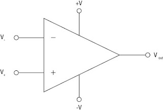
Schematic symbol for an Operational Amplifier

The signals are applied to the V+ and V- terminals.  The supply voltage is applied to the +V and -V terminals and the output is seen at Vout.  The triangle is used to signify amplification.  Wherever you see a triangle like this in electronics or in flow diagrams it's to show amplification.

Op-amps is a very large and diverse topic and going through everything in one blog post isn't possible....I wish it were so simple!  So really how do we use these things?  Ok there are formulae and datasheets and a few things we need to know before we can design a circuit.  Lets set the design parameters and then get started:

What kind of signal are we needing to amplify? Fast, slow, large, small, alternating etc  By fast or slow what I'm really asking is how fast does the amplifier need to react to a change.  This is known as Slew Rate.  Large or small means Input Voltage range and alternating really means frequency range of operation or Bandwidth - as in how often will the signal applied to the inputs repeat.  It is also important to know how much supply voltage we need and whether the device is single rail or dual rail operation.  An example of single rail is a device that can work with 0V on the -V terminal and +5V on the +V terminal.  Dual Rail would mean -5V on the -V terminal and +5V on the +V terminal.

So lets recap on the most important parameters that we need to look at for selecting a device:

Size of signal to amplify - Input Voltage Range
Frequency of signal - Bandwidth
Size of Supply - Voltage Supply
Amount of Gain required -

For an example I'm going to use the UA741 Op-Amp - it's the most popular and most people will be familiar with it.  Here is the datasheet:

http://www.ti.com/lit/ds/symlink/lm741.pdf

Let set some parameters for an example.  Lets say we want to amplify a 1kHz 0.5V AC signal - like say the output from a microphone or something.  Lets say we want to use a +/-5V supply and that we want the output signal to be bigger lets say 5 times bigger!

The first thing I would do is check the datasheet to make sure that this Op-Amp can do all of those things - don't worry it can!

Here is the circuit:

741 Non inverting Amplifier with no gain
 What this circuit will do is take the 0.5V pk-pk signal applied to the V+ or non inverting terminal and try to amplify it as much as possible!  It can only get as big as the supply voltage applied though to the output will be 5V pk-pk.  The output signal will also be clipped because we are not controlling the amount of gain we require.  Check out the oscilloscope screen!

741 Non Inverting amplifier with no Gain Oscilloscope Output - Blue = Input, Red = Output
What this shows is that the signal is being amplified and it's in phase but we are losing part of the signal integrity because we are cutting off the top and bottom of the wave.  If the input signal shape was important we couldn't use this circuit as we have lost information (how big was the signal etc).

It's better to control the amplifier so that we can tell how much our input signal is going to be amplified so we don't lose part of the signal and we can be sure that all the signal information at the input is present at the output.  We do this by setting the gain of the amplifier and there are two very important formulas that any aspiring electronics engineer needs to know:

Av (Gain) = Vout / Vin or Av (Gain) = - Rf / R1 for an inverting amplifier

Av (Gain) = 1 + Rf / R1 for a non inverting amplifier

A non inverting amplifier is a circuit where the signal is applied to the V+ terminal (pin 2 on a uA741) and an inverting amplifier is where the signal is applied to the V- terminal (pin 3 on a uA741)

The gain of an amplifier is set by choosing to place resistors around the op-amp circuit so that part of the signal at the output is fed back to the input reducing the output signal and getting a more stable lower voltage response.  Lets check out an inverting amplifier with a gain of ten:

uA741 Inverting Op-Amp with a Gain of Ten
Before we show the oscilloscope output lets do a quick bit of mathematics - Lets plug the values into the formula and prove we will get the gain of ten.  The circuit is a standard circuit for an inverting amplifier.

Av = - Rf / R1

Rf = 10k Ohms or 10,000 Ohms
R1 = 1k Ohms or 1000 Ohms

Therefore Av = - (10,000 / 1000)
Av = - 10

The hyphen '-' shows that the amplifier is inverting

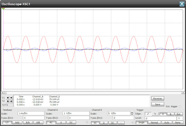
So the maths show that this amplifier will try to amplify the signal at the inverting terminal to ten times it's current size (voltage).  Check out the oscilloscope screen:

Inverting Amplifier with ten times gain - Red = Output and Blue = Input
The oscilloscope screen shows that we are getting a bigger signal at the output and the more observant viewer may notice that the signal is 180 degrees out of phase with the input or it's been inverted.  The signal is still being clipped so we are over amplifying our input signal. We can fix this by either reducing (attenuating) the input signal so it's smaller or increasing the supply voltage so that the Op amp is not 'running close to the rails'.  Lets do both and see what happens:

Inverting Op-Amp with ten times gain and no clipping

I have now changed the input signal to 0.1V and the supply voltage is now +/-12V so the signal will not clip but the gain of the op-amp will still be ten.  Here is the oscilloscope output:

Inverting Op-Amp with ten times gain and no clipping
So now we have a perfect output signal with no clipping and the signal is faithfully reproduced but inverted.  If we wanted a signal that was not inverted we need to use a slightly different circuit helpfully called the non-inverting amplifier.  Here is the circuit:
Non Inverting Amplifier with a gain of 11

Lets do the maths again and see what that the gain is set to 11 this time!

AV = 1 + Rf / R1

AV = 1+ (10000/1000)

AV = 11

Just for completeness lets check out the oscilloscope output just to show that this true and what the signal will look like:

Oscilloscope output of the Non-Inverting Amplifier
Well that's about it for inverting and non inverting Op-Amps.  The reason you might choose to use an inverting amplifier over a non inverting amplifier is because the bandwidth response of an inverting amplifier is better over a longer range.  That means that you could use the amplifier with a better range frequencies of input signals.

We are going to use an Op-Amp in the AD9835 Signal generator project and the next post will go through the design of that section of the project.  I will add some video showing the actual circuits working.

Take care people! - Apologies for the really long post!

Tuesday 16 October 2012

Filter for the AD9835 Function Generator

In the last post I used the AD9835 Breakout board from Sparkfun.  I'm going to use it to make a function generator for my local hackspace and probably one for my own bench too.  I could buy one but that doesn't get me loads of content for the blog and I think I can add some value by adding features that aren't available on some Bench Function Generators.

A quick search on Ebay showed that good function generators on Ebay cost around £200.  I think I can do a little better with the one I'm designing but we shall see.....There are some awful ones for a lot less and If I was in a real hurry I might consider buying one.  Buying test equipment is always a problem for engineers and hobbyists alike.

The Sparkfun AD9835 breakout board cost £26.46.  I don't think that's too bad a deal.  It was quick to get up and running and produces a pretty good sine wave.  I like the fact that I can use it with my arduino and it's a great learning project as to make a full function generator will use a lot of different electronic techniques to achieve what is required.

And now back to the Function generator...

The one thing that isn't provided on the AD9835 breakout board is a filter.  Why does it need a filter? Well.....you could use it as is without one but prolonged use will show that it's output is tainted with the 50MHz source clock coming from the reference oscillator on the breakout board....That sounded very technical!  What does that mean?  The tainted bit means that the sine wave at the output will look very square and choppy at certain frequencies because of interference from the reference clock. In order to get the AD9835 DDS chip to work it needs a 50 MHz reference clock which is a square wave pulse which oscillates (changes state from High to Low) every 0.00000002 seconds or 20 nanoseconds.   It is better to have what is known as a spectrally pure output which is an output with only the signal we want and not the 50 MHz reference clock.  

Oscilloscope Screenshots showing the output of the AD9835 when it's output hasn't been filtered. 
If we look at the output of the breakout board in terms of frequency instead of time by using a spectrum analyser we can more easily visualise the problem.  A spectrum analyser is a special piece of test equipment quite like an oscilloscope that shows a graph electronic signals with volts on the 'y' axis and frequency on the 'x' axis.  It's a piece of test equipment that RF engineers use all the time.  I wish I had my own sometimes!  I have the use of a couple at work...which is helpful.

Spectral Output of the AD9835 when unfiltered.  
In order to get a spectrally pure output we are going to have to add what is known as a low pass filter to the output of the AD9835 breakout board.

Electronic Filters are special circuits that are used to purify electronic signals.  It's a way of removing the parts of the signal we don't want leaving the information that we do want.  A real world example of a filter is a pair of sunglasses.  We don't want our eyes to be dazzled by bright light so we filter the bright light out using some darkened lenses.

Anyway the AD9835 breakboard needs a filter to remove the 50 MHz reference clock.  When I specified what I wanted the function generator to do I specified that the frequency output range needs to be from 1 Hz to 10 MHz.  This being the case we can now design a filter that allows all signals to pass through the filter up to 10 MHz but completely blocks any signals above 10 MHz.  To  give us some margin I'm going to design the filter to cut off (stop allowing signals through) at about 15 MHz - this is known as the corner frequency.  The filter is known as a 'Low Pass Filter' - this is because it allows low frequency signals through but blocks (attenuates) high frequency signals.  Other types of filters are available including High Pass, Notch, Bandpass etc.

Filters is a huge subject in electronics and there are several thousand books and tutorials on the subject.  There are so many different types of filter that I can't cover them all here.  If people need more information on filters then the following sites might be of some help:

http://en.wikipedia.org/wiki/Filter_(signal_processing)
http://www.allaboutcircuits.com/vol_2/chpt_8/1.html

For the AD9835 breakout board I'm going to design a passive filter known as a 'Chebyshev' filter.  It is a passive filter made of inductors and capacitors.  It's called Chebychev because it uses polynomials found the by the Russian Mathematician Pafnuty Chebyshev.  The mathematics involved are incredibly complicated.  I'll be honest....I didn't go through it all and do lots of Maths.  I used an online filter calculator like this one:

http://www.wa4dsy.net/filter/hp_lp_filter.html

I used the one built in to National Instrument's simulation software - Multisim.  It came out with the following circuit.  I changed the values to suit what I had available.

AD9835 Filter circuit with values

Ignore the 0V DC source - its present to allow me to simulate the circuit.  What I'm going to simulate is what will happen at the output of this circuit if we place a sine wave at Vin with a frequency from
1 Hz to 50 MHz.  This is where circuit simulators are very useful as they can tell the design engineer how a circuit is going to respond before building it.  It gives confirmation as to what should happen. Simulators are also very useful because you can change component values and see what that changes to the circuit's function.  All good design engineers should use simulators - it's the best way to quickly check the function of a circuit.


So here is the result of a frequency sweep from 1 Hz to 50 MHz:


Chebychev Filter using 4.7uH Inductors and 100pF Capacitors
The top graph or trace shows the filter response.  If a 1 V sine wave is placed at the input with a frequency less than 12 MHz the signal will not be reduced or attenuated in size.  If the signal is above 12 MHz it will drop in magnitude at the rate indicated by the slope of the graph.  

The lower trace is the phase relationship between the input signal and the output signal.  What that means is that at around 7 MHz the phase between the input signal and output signal reverses.  In our case this doesn't really matter but it might be of interest if you need to ensure that the input signal is always in phase and not reversed (audio circuits....perhaps).

So....if we construct this filter carefully using the above components and a sensible PCB layout we will get the above response.....Well guess what I did and here it is:


The above screen shot seems to correlate quite nicely with the trace from the simulation.  This means that the filter works and my layout was sufficient to provide the correct response.  Not bad seeing as that was incredibly rushed and I paid no attention to component placement!  Sometimes I'm lucky!

Here is a video showing the testing:


I wish I could afford a Vector Network analyser for my own nefarious purposes!  For some reason my missus won't let me buy one...at £25000 I suppose I understand!  Vector network analysers are a very specialised piece of electronics instrumentation used for assessing the frequency response of electronic circuits and cables.  The one I used in the above video has a frequency range of 100 kHz to 8 GHz!  We use it at work for testing antennas, filters, amplifiers and coaxial cables.

So now that we have proved this part of the design, I'm going to add this filter circuit to the output of the AD9835 breakout board.  This will prevent the reference clock interfering with the output.  The next part of the circuit to design will be the amplifier stage.  

Cheers for reading - take care

Alex
    

Sunday 14 October 2012

Function Generator - AD9835 Based

The last few posts have been on the applications of transistors and how to use them in circuits.  I was trying to make some video footage of those circuits in action when I realised I haven't got access to a suitable function generator!  I have a couple of cheap circuits that I made from kits years ago but they aren't really suitable for lab based bench work.

So I have decided to make one!  I'm hoping to use this project to re-learn some of the electronics theory I have forgotten and share it with everyone else so that someone else can benefit from my efforts.  Its a win win!  I get a function generator for my efforts and the people who bother to read this get to learn a little bit about electronics and how some instrumentation is designed....At least that is the plan.

A function generator for those that don't know is a piece of electronic equipment that simulates electronic signals.  These signals can be sine waves, square waves, ramp waves or pulses or an arbitrary electronic signal of some kind.  The output frequency and voltage can be varied as required.

Electronics engineers use these devices to test different types of electronic circuits including:

Audio Amplifiers
Signal or Instrumentation Amplifiers
Electronic Filters - all different types

So here goes....lets list the kind of features for the function generator that we need or want.

Sine wave output
Square wave output
triangle wave output
Monostable pulse output
Voltage variable from 0V to 5V
Frequency variable from 1Hz to 10MHz
Software control of instrument from a computer

Building a piece of equipment like this from scratch is a lot of work....However if we break the problem up into sections we can make things easier for ourselves.

Block Diagram of Function Generator
The sections highlighted in blue show the inputs section and and the red highlights the output.  Technically the filter and microprocessor section are in the processing section but it doesn't really matter.  All systems are built up of input stages, processing stages and output stages.

Anyway...so for our function generator we need a way of generating waveforms and a microprocessor to control it and some way of interacting with the microprocessor to tell it which wave we want (sine, square or triangle), how big it needs to be (Voltage) and how often the wave repeats (Frequency).

So the first part of the diagram we need to make is the wave generator.  There are thousands of different circuits for doing this and all of them have their place.  Look in any electronics text book or online encyclopaedia for oscillator and you will find mention of a waveform generator circuit.  One of the more popular circuits is called a Wien Bridge Oscillator.  The modern circuit is based on a very popular Master's thesis by some bloke named William Hewlett.  He went on to form Hewlett Packard and became incredibly famous and rich!  Here is the wikipedia entry:

http://en.wikipedia.org/wiki/Wien_bridge_oscillator

But I'm not going to make a Wien bridge oscillator for this function generator.  I'm using a component from Analogue Devices called a Direct Digital Synthesis (DDS) generator.  The one I'm going to use is the AD9835 and here is the datasheet:

http://www.analog.com/en/rfif-components/direct-digital-synthesis-dds/ad9835/products/product.html

The reason I'm going with this device is because it comes already laid out on a breakout board from Sparkfun Electronics, although I bought mine from Proto-Pic

http://proto-pic.co.uk/breakout-board-for-ad9835-signal-generator/


I like this breakout board for two reasons.  It has a good frequency output range from 1Hz to at least 25MHz and it is easy to control via the arduino.  The reason this is the case is because an excellent library has been written to make the control very simple!  It was written by Lachlan Gunn and can be downloaded here:

https://github.com/LachlanGunn/Synthesis

It's an excellent library.  I wish I had the programming skill to write similar libraries.  So having downloaded the library and read the instructions and made the connections specified, I switched everything on....It worked straight out of the box!  Here is the obligatory youtube clip showing it working!


In order to properly use the DDS breakout board we will need to filter out the fundamental 50MHz clock signal which is on the breakout board.  The next post will be on filters!  If people would like to know how the AD9835 device works then this is the site for you:

http://alternatezone.com/electronics/dds-art.htm - Kudos yet again to David Jones of the EEVblog.

Check out all of his stuff and his videos here: EEVBlog

Best of luck and enjoy - Langster!


Monday 1 October 2012

How do you use PNP transistors


So last post dealt with NPN transistors and now I show how to deal with the PNP Transistor.

How do you use NPN Transistors

PNP transistors are in essence exactly the same as an NPN transistor but they work in a complementary or mirrored fashion.  So rather than applying 0.7V to the base terminal to get the transistor to conduct in this case we need to apply (at the base terminal) 0.7V less than the voltage at the emitter.  The diagram below shows how a PNP transistor is used:


PNP transistors are used where the circuit needs to control a part of the circuit connected to the 0V side or where 'high side' control is required.  PNP transistors are again used as a current amplifying device or as a switch.  Unlike NPN transistors these devices are 'active low' and that means they start to turn on when the voltage at the base is reduced.  They were popular in the early days of electronics because they had a lower noise characteristic and they could switch on and off more quickly. Early electronics design engineers used them in radio circuits and high speed switching circuits.  They aren't quite so popular these days as NPN transistors have improved and there is not such an appreciable difference between them.  Below is the wikipedia entry for transistors covering all the aspects in detail:

http://en.wikipedia.org/wiki/PNP_transistor#PNP

Many electronics engineers I know struggle to use PNP transistors because during their training PNP transistors were not covered properly.  I know this was the case for me and it's part of the reason I write these blog posts, it's my effort to try to redress the balance.  NPN transistors were covered very clearly and we were taught that PNP transistors were the same only in reverse.  Technically this is true although I didn't find this obvious at all.  I think a better description is that PNP transistor operation is the 'mirror' of NPN transistor operation.

How do you use a PNP transistor? 

Well....in my opinion it isn't the same process as designing a circuit with the NPN Transistor!  So here we go: to use the transistor connect the emitter to the supply voltage and the collector to the low side of the circuit or the '0V' rail.  Next to turn the transistor on and cause current to flow through the transistor we need to apply 0.7V less than what is present at the emitter.  Check out the circuits below:

Left : PNP Transistor Circuit with Voltmeters, Right: PNP Transistor Circuit with Ammeters

As with the NPN transistor we can see that the current flowing at the base is less than the current flowing at the emitter so we have current amplification as before.  The amount of 'gain' or amplification is again dependent on the transistor's Hfe parameter.  The datasheet for the BC558 transistor is below.  I chose this transistor as it is the PNP compliment of the BC548 NPN transistor I posted about previously.  All of the resistor values are also the same to be consistent.  


If we look at the circuit closely and compare it with the NPN version we can see that the circuit isn't the reverse of the NPN transistor but the mirror or complement.  This is why the BC558 transistor is called the BC548 complement.  


Just for completeness let's calculate the Hfe from the measurements in the circuit above.

Hfe = Ic / Ib

Hfe = 2.532*10^-3 / 0.013*10^-3

Hfe = 194.77 - lets round this up to 195 

If we now look at the datasheet for the BC558A we can see the manufacturer specifies an Hfe of 110 to 220.  Yet again we are within specification!

So what parameters do we need to know to be able to use a PNP transistor.  They are pretty much the same as the NPN transistor but they are quoted with a minus sign to denote that it must be less than the supply voltage.

VCEO - Collector Emitter Voltage - Maximum Voltage you can place at the emitter
VCBO - Base Collector Voltage - Maximum Voltage you can place at the collector
VEBO - Base Emitter Voltage - Maximum Voltage you can place at the base

Ic - Collector Current - Maximum current you can cause to flow through the transistor from the supply

Pc - Power dissipation - Amount of power the transistor will dissipate when fully on

How do we use a PNP transistor as a switch?

Let use a PNP transistor to control an LED.  Lets set the supply voltage to 12V and then use a control voltage to turn the transistor ON and OFF.  Here is the circuit:
The resistor on the base is a current limiting resistor to prevent too much current being applied to the base terminal.  When the base voltage is set at 12V the LED is not on.  Check out the video below to see the circuit simulation in action:

Hope this video makes sense to everyone.  It shows very clearly that you can have very precise control of when an LED or relay was activated if you were to use a PNP transistor as a switch.  It's a lot easier to reduce a voltage precisely from high to low than it is from 0V to high.

How do you use a PNP transistor to Amplify?

In the previous post I made a Class A amplifier using an NPN transistor.  Here is the complimentary circuit using a PNP transistor.  It's not a practical circuit by any means but it does show the principle of a PNP transistor as an Amplifier.  In practice most amplifiers are made up of a combination of NPN and PNP transistors.  This is a topic for another post though!

Here is the circuit for the PNP Class A Amplifier:


As can be seen the circuits component values are exactly the same as the previous NPN circuit only everything has been 'mirrored'.  The transistor has been 'biased' ON using the voltage divider of R1 and R2.  The gain of the circuit is set with R3 and R4 at a gain of 6.  We are using a 1kHz 0.5V AC for our input signal.

Here is a video simulation of the circuit in action:


That's all for now!  If anyone would like more posts on transistor usage please let me know in the comments section,

Cheers

Alex