The original circuit and some very good documentation and kits are available here:
MintyBoost V3.0 - Very cool stuff from Adafruit Industries!!!
The circuit is a switch-mode dc to dc converter. I haven't talked about switch-mode power supplies before so here goes! This might get complicated....bear with me!
Power supplies can be realised in several different forms:
Step UP - Increase voltage or current
Step Down - reduce voltage or current
ac - alternating current
dc - direct current
Linear - conversion in a straight line...see previous posts
Switch-mode - use a combination of an inductor, zener diode and capacitor to provide a different voltage than the input.
Switch-mode power supplies are based on an electronic trick...What they do is take energy in one form and convert it to another form to get the desired output. How they work is they take a dc voltage source (input) convert it to a pseudo alternating signal (square wave or pulse width modulation) and pass that signal through a combination of an inductor, switching diode and capacitor. The way the inductor diode and capacitor are connected denotes the type of switch-mode power supply. This is known as the switch-mode topology....Some examples of these are:
Buck (Step Down)
Boost (Step Up)
Flyback (Step Up)
A Buck regulated switch-mode power supply (SMPS) would take in say 12 V and give out 5 V at a steady current.
A Boost regulated SMPS takes in say a 3 V input and boosts it to 5 V
The circuit topology depends on how much power or energy the circuit designer requires. SMPS are popular because they are more efficient than linear power supplies and use smaller and cheaper components. The drawback of switch-mode power supplies is that they have inherent electronic switching noise which can affect sensitive instrumentation circuitry.
Wikipedia has a great entry on how boost converters work:
http://en.wikipedia.org/wiki/Boost_converter
Here is a quick example simulation I made up just to show how boost converters work. Essentially what they do is increase the output voltage by taking the input voltage, creating a switching waveform and passing that signal through an inductor, switching (Schottkey) diode and a large electrolytic capacitor. By doing this the energy in the switching waveform is held as magnetic energy in the inductor for a very short period of time. This energy then charges the capacitor up. When the switching waveform changes polarity the energy in the capacitor is dumped to the output...this energy dumping is seen by the output as an increased voltage. The classic water analogy would be filling a large water tank very quickly with low pressure and then emptying it all in one go giving the impression there is more water pressure present at the output than at the source.
Here is the circuit:
Here is a simulation video showing the various parts of the circuit and the switching and output waveforms on an oscilloscope.
The section containing the signal generator and the TIP41CG transistor can be combined into a single integrated circuit called a boost converter. The IC used in the circuit by Adafruit Industries in the mintyBoost was an LT1302 micropower Boost Converter. Its a very useful device if a little expensive! It basically combines the chopper signal generator and switching transistor into one single device which is easy to use.
LT1302 product page
Here is the schematic diagram for the Adafruit minty Boost....I have redrawn it for my own nefarious purposes. The component values and types are exactly the same as Adafruit used.
Here is my PCB layout. It uses a single sided PCB to make it easy to etch using the toner transfer method
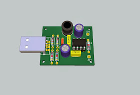
Just for fun I rendered the PCB in google Sketchup to show how the device will look once I have populated
Here it is again with a 2xAA battery holder and some mechanical dimensions - Renders are Cool!
Anyway....I made the circuit for real....for once it worked first time! I am not surprised however as all of the hard work was done for me by Limor Fried of Adafruit industries....they do excellent work - Please check them out!
Here is a picture of the realised circuit! The photograph is of a previous version I made with the PCB elongated to hold the battery compartment. I decided to shorten the PCB for this version to reduce costs!
That's it for now. Enjoy - Langster!


No comments:
Post a Comment