It's been a while since I wrote anything up and to be honest with you I haven't had much time or inclination to do any electronics outside of work....it gets that way sometimes.
Here is the previous post on this project for those that are following along:
http://langster1980.blogspot.co.uk/2017/05/graphing-data-from-venturi-tube.html
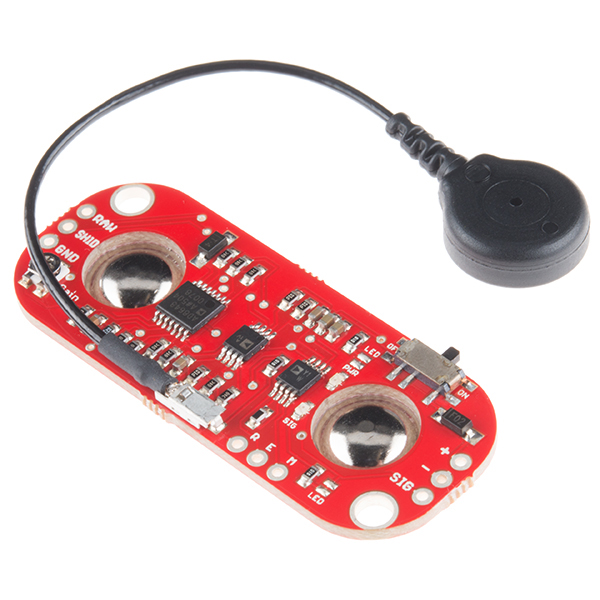
I received in the post a Myoware EMG (Electromyography) sensor kit available from Sparkfun and other vendors. The webpage for the product is shown below:
https://www.sparkfun.com/products/13723
The idea with this circuit is to sense muscle movement when a person breathes in and out and from that correlate lung function. How much air a person can breathe in and out is partly to do with muscle (diaphragm) and chest movement - I'm not a medical doctor so I'm a little out of my depth here...however it was part of the functionality requested for the medical device so I'm investigating solutions and this circuit is one solution. Lets see how well it works and get some data and compare it to what would be expected. As a healthy male of some 30+ years (in my prime!) it should show that I'm a paragon of excellence...in reality I suspect it will show that my heart and muscle function are average but more importantly present!
Here are the instructions for use:
https://github.com/AdvancerTechnologies/MyoWare_MuscleSensor/blob/master/Documents/AT-04-001.pdf
The board itself is very simple to setup and use and the instructions are clear and concise.
This is the setup I'm going with...I'm certain there shouldn't be any issues but I don't have the buffer circuit so...it's time to man up!
I have attached the red sensor wire and blue sensor wires to electrode pads and put them on my sternum at either side of my heart. I attached the black wire to an electrode pad and placed that on my stomach to provide a base reference. I'm looking to measure my hearts sinus rhythm...and see how sensitive things are. Here is the test code I've written:
(I had both the raw and sig output connected to my arduino analogue inputs A0 and A1)
//test code for Myoware EMG PCB
// variables for input pin from MyoWare PCB
int analogInputSig = A0;
int analogInputRaw =A1;
// variables to store the values
int valueSig = 0;
int valueRaw = 0;
void setup() {
pinMode(analogInputSig, INPUT);
pinMode(analogInputRaw, INPUT);
// begin sending over serial port
Serial.begin(9600);
}
void loop() {
// read the values from the sensor:
valueSig = analogRead(analogInputSig);
valueRaw = analogRead(analogInputRaw);
//print the reading received
Serial.print(valueSig);
Serial.print(",");
Serial.print(valueRaw);
Serial.println();
// wait for a bit to not overload the port
delay(10);
}
Here is the serial output graphed for your viewing pleasure:
Here is my wife's heart rate...apparently I don't have quite the effect on her I used to!
Here is what happens when the sensors are placed on the abdomen:
So...I'm alive and so is the wife! The Myoware picks up a good strong electrical signal when sensors are placed close to the heart...but when placed on the abdomen did not really pick up anything I could see correlating to breathing or diaphragm movement. Either I had my sensors incorrectly placed or the circuit is not sensitive enough for this purpose. Adjusting the gain potentiometer on the Myoware PCB did change the gain response but didn't provide the response I was looking for - It was hoped that it would be possible to correlate diaphragm muscle movement with regular breathing.
I did notice that if I activated (flexed) my abdmoninal muscles electrical signals were definitely present and well detected...maybe I don't use my diaphragm much when I breathe in and out? I will have to investigate further.
I could not find a schematic diagram for the Myoware circuit although the shields are marked as being open source. Update - See comments below from Brian Kaminsky of Advancer Technologies.
Here is the schematic for the previous version of the device:
https://cdn.sparkfun.com/datasheets/Sensors/Biometric/Muscle%20Sensor%20Platinum%20v3.3.pdf
The main integrated circuit is an AD8648 which is a quad operational amplifier. I suspect the two smaller devices are programmable gain devices for each of the sensor inputs and the rest of the components are associated gain and filtering requirements.
Here is the datasheet for the AD8648
http://www.analog.com/media/en/technical-documentation/data-sheets/AD8646_8647_8648.pdf
Here is the datasheet for the devices marked AD A 1V (An AD 628 I think....)
http://www.analog.com/media/en/technical-documentation/data-sheets/AD628.pdf
The company (Advancer Technologies) that developed the Myoware PCBs also wrote this instructable which shows how a similar circuit could be developed:
http://www.instructables.com/id/Muscle-EMG-Sensor-for-a-Microcontroller/
I have seen similar circuits in the past and believe this is certainly one route to achieving the measurement of electrical signals either from the heart (ECG - ElectroCardioGrapy) or muscle movement (EMG - ElectroMyoGraphy).
I would certainly say that this circuit has been very well designed and implemented and would be very useful if one wanted to use muscle flexing signals to control an external device or detect when someone has used a muscle...so say for instance you wished to mirror your arm movement with a robotic arm then this is definitely the circuit for the job!
That is all for now - take care always, Langster!
Wednesday, 21 June 2017
Thursday, 8 June 2017
Tutorial for Xilinx DCM Clock Generator with the Mimas V2
A blog reader contacted me recently for help generating signal clock sources with the Mimas V2. In particular they wanted a 108 MHz clock for HDMI purposes however the Spartan 6 FPGA on the Mimas V2 is capable of generating source clocks up to 1 GHz if the output is used to drive a BUFPLL. What this means is that the clock will be generated but in order to work special internal routing is required within the FPGA. It is a topic for another post to be honest. For now lets only generate clocks up to 400 MHz
The datasheet for the the Spartan 6 FPGA devices is available below:
https://www.xilinx.com/support/documentation/data_sheets/ds162.pdf
Rather than write a lot of VHDL code to generate the clocks we need we are going to use a feature of Xilinx WebISE 14.7 to write the code for us - cool huh.
Lets set some parameters! Lets generate a 200 MHz clock and send it to one of the output pins and then view this on an oscilloscope or logic probe. If people are interested the instruction manual for the DCM clock generator is here:
DCM Clock Generator Manual
Lets fire up Xilinx WebISE and start a new project:
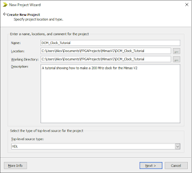
Choose to save the project in a suitable location on your hard disk and give the project a suitable name - I called mine DCM_Clock_Tutorial but any sensible name will do:
Click Next when ready.
Make sure all the settings are the same as in the image below - these are the settings required for the FPGA device on the Mimas V2:
Click Next when ready to display the project summary page:
And finally click Finish to return to the main project screen:
Now right click on the design hierachy window and select add source:
Select VHDL module and give the file a suitable name, I called mine DCM_Clock_Top_Module but another name could be used. It should be something sensible however:
Click Next to continue and add the inputs and outputs. I have chosen to add a signal called CLK as an input and a signal called CLKOUT_200M as an output. If we wanted to we could leave this screen blank and write our own code later.
Click Next to continue and display the summary screen:
Click finish to return to the main project window and see the automatically generated code:
I prefer to delete most of the comments as they don't add any value at this point however...they can be left or completed if required.
At this point it is always a good idea to save things.
We will return to write VHDL code here later but for now lets add another new source, this time select IP (Core Generator and Architecture Wizard) and give the file a suitable name:
Click Next when ready and then wait for WebISE to load up all of the available IP cores for the Spartan 6 family:
Type Clock into the search field:
Click Next when ready:
Click Finish and wait for WebISE to build the code and load the wizard.
Make sure the settings are as shown below:
The options selected are for the Mimas V2 which has a 100 MHz source clock. We have also chosen to reduce jitter which should make the clock more accurate and we have decided to let WebISE select the most applicable mode for us - Click Next when ready to continue:
Ensure the same settings have been selected and click Next when ready.
Ensure the settings are the same as above and click Next when ready - for this tutorial we don't need a reset input or locked input.
These are the IO functions which will be automatically created by the wizard when the code is generated. Click Next when ready.
These are the names that will be used for the input clock signals and output clock signals - Click Next when ready.
Click Generate when ready and wait until the code has been generated.
Now here is where we could do things in multiple ways. We could add code to the VHDL module or we can take advantage of WebISE and have it write the code for us...I'm going to take the easy option. Click on the newly created ClockMultiplier200M module in the Hierachy Window and then expand the CORE Generator process icon and select View HDL Instantiation Template:
Open the file and scroll down to line 67:
Select and copy the VHDL code from line 67 to line 76:
Paste this code into the VHDL top module code at line 11 in the header of the architecture function:
Now return to the HDL Instantiation Template and select the code on line 82 to line 89 and copy it. Then paste that code into the top module code on line 22 between the begin and end Behavioural lines:
Go to line 22 and change the text 'your_instance_name to something sensible, I typed clockMultiplier:
Next we need to modify the code so that the port map section connects to the inputs and outputs in the Entity section:
Next we need to generate the implementation constraints file. Right click on the hierarchy window and select Add new source like before:
Click Next when ready.
Click Finish when ready.
We need to create the implementation constraints code specifically for the Mimas V2. I tend to use the original supplied by Numato Labs and then modify it to suit our purposes. Copy and paste the code below into the text editor in WebISE:
#******************************************************************#
# UCF for Mimas V2 # # #
#******************************************************************#
CONFIG VCCAUX = "3.3" ;
NET "CLK" LOC = V10 | IOSTANDARD = LVCMOS33 | PERIOD = 100MHz ;
NET "CLKOUT_200M" LOC = T10 | IOSTANDARD = LVCMOS33 | DRIVE = 8 | SLEW = FAST | OUT_TERM = UNTUNED_50 ; #Pin 4
The above code tells the 'compiler' that the CLK input from the 100 MHz crystal oscillator is connected to pin V10 and that we would like to use pin T10 as the 200 MHz output pin on P8 pin 4. The pin has been set to provide a 50 Ohm output impedance. I chose the T10 pin as according to the information in ug381.pdf (The DCM Clock Manager Manual) this pin - GCLK2 is a global clock pin location.
I chose to set the impedance to 50 ohms so that it can be properly measured with an oscilloscope.
The datasheet for the the Spartan 6 FPGA devices is available below:
https://www.xilinx.com/support/documentation/data_sheets/ds162.pdf
Rather than write a lot of VHDL code to generate the clocks we need we are going to use a feature of Xilinx WebISE 14.7 to write the code for us - cool huh.
Lets set some parameters! Lets generate a 200 MHz clock and send it to one of the output pins and then view this on an oscilloscope or logic probe. If people are interested the instruction manual for the DCM clock generator is here:
DCM Clock Generator Manual
Lets fire up Xilinx WebISE and start a new project:
Choose to save the project in a suitable location on your hard disk and give the project a suitable name - I called mine DCM_Clock_Tutorial but any sensible name will do:
Click Next when ready.
Make sure all the settings are the same as in the image below - these are the settings required for the FPGA device on the Mimas V2:
Click Next when ready to display the project summary page:
And finally click Finish to return to the main project screen:
Now right click on the design hierachy window and select add source:
Select VHDL module and give the file a suitable name, I called mine DCM_Clock_Top_Module but another name could be used. It should be something sensible however:
Click Next to continue and add the inputs and outputs. I have chosen to add a signal called CLK as an input and a signal called CLKOUT_200M as an output. If we wanted to we could leave this screen blank and write our own code later.
Click Next to continue and display the summary screen:
Click finish to return to the main project window and see the automatically generated code:
I prefer to delete most of the comments as they don't add any value at this point however...they can be left or completed if required.
At this point it is always a good idea to save things.
We will return to write VHDL code here later but for now lets add another new source, this time select IP (Core Generator and Architecture Wizard) and give the file a suitable name:
Click Next when ready and then wait for WebISE to load up all of the available IP cores for the Spartan 6 family:
Type Clock into the search field:
Click Next when ready:
Click Finish and wait for WebISE to build the code and load the wizard.
Make sure the settings are as shown below:
The options selected are for the Mimas V2 which has a 100 MHz source clock. We have also chosen to reduce jitter which should make the clock more accurate and we have decided to let WebISE select the most applicable mode for us - Click Next when ready to continue:
Ensure the same settings have been selected and click Next when ready.
Ensure the settings are the same as above and click Next when ready - for this tutorial we don't need a reset input or locked input.
These are the IO functions which will be automatically created by the wizard when the code is generated. Click Next when ready.
These are the names that will be used for the input clock signals and output clock signals - Click Next when ready.
Click Generate when ready and wait until the code has been generated.
Now here is where we could do things in multiple ways. We could add code to the VHDL module or we can take advantage of WebISE and have it write the code for us...I'm going to take the easy option. Click on the newly created ClockMultiplier200M module in the Hierachy Window and then expand the CORE Generator process icon and select View HDL Instantiation Template:
Open the file and scroll down to line 67:
Select and copy the VHDL code from line 67 to line 76:
Paste this code into the VHDL top module code at line 11 in the header of the architecture function:
Now return to the HDL Instantiation Template and select the code on line 82 to line 89 and copy it. Then paste that code into the top module code on line 22 between the begin and end Behavioural lines:
Go to line 22 and change the text 'your_instance_name to something sensible, I typed clockMultiplier:
Next we need to generate the implementation constraints file. Right click on the hierarchy window and select Add new source like before:
Click Next when ready.
Click Finish when ready.
We need to create the implementation constraints code specifically for the Mimas V2. I tend to use the original supplied by Numato Labs and then modify it to suit our purposes. Copy and paste the code below into the text editor in WebISE:
#******************************************************************#
# UCF for Mimas V2 # # #
#******************************************************************#
CONFIG VCCAUX = "3.3" ;
NET "CLK" LOC = V10 | IOSTANDARD = LVCMOS33 | PERIOD = 100MHz ;
NET "CLKOUT_200M" LOC = T10 | IOSTANDARD = LVCMOS33 | DRIVE = 8 | SLEW = FAST | OUT_TERM = UNTUNED_50 ; #Pin 4
I chose to set the impedance to 50 ohms so that it can be properly measured with an oscilloscope.
Lets save our work and upload it to the FPGA - Click on the implement top module arrow button and then after those processes are complete create a bitfile. Navigate the to folder where the project was stored and locate the newly created bitfile! Then load up the MimasV2 Configuration tool and connect up your Mimas to your PC. Select the appropriate COM port and then....
Then upload it to the Mimas V2 development board:
Once uploaded Pin 4 of the output Bank P8 should have a clock signal on it which can be viewed with an oscilloscope or logic probe. In truth these clock signals are designed to be used internally within your FPGA design and not brought out to a pin. The signal won't be particularly square or have a a fast rising edge.
Here is a photo I took of a signal from the FPGA measured with an oscilloscope - it looks more like a sine wave!
That's all for now - Langster
Here is a photo I took of a signal from the FPGA measured with an oscilloscope - it looks more like a sine wave!
That's all for now - Langster