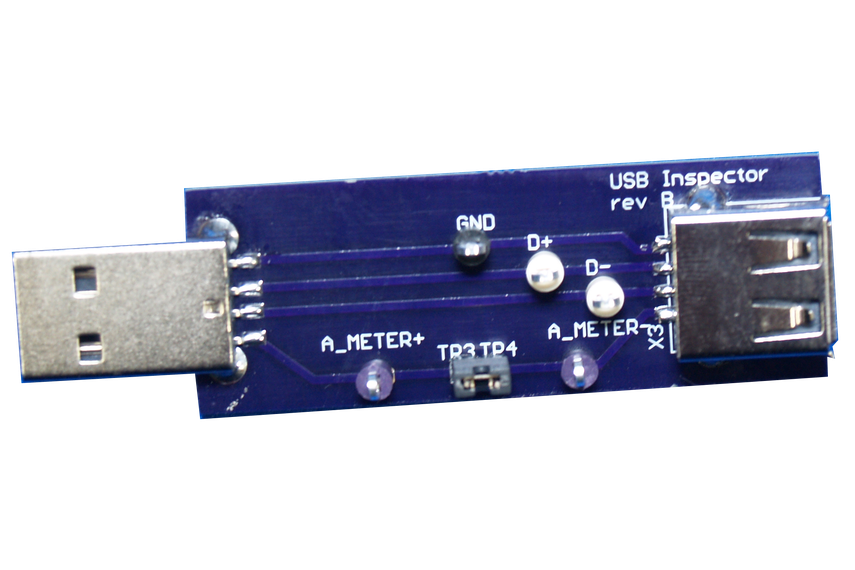
 |
| Image Copyright - Misperry via Tindie |
https://www.tindie.com/products/misperry/usb-inspector/?pt=full_prod_search
I also found this product on tindie which is similar but has a current monitoring circuit built in:
https://www.tindie.com/products/Kaktus/usbuddy-usb-development-tool/?pt=full_prod_search
A friend of mine and blog reader found this one:
https://friedcircuits.us/50?search=usb
Either of these products would work for my purposes but the first product's shipping costs from the USA seem a little extravagant and I only wanted one or two.
The second product uses pin headers to allow connection which are a bit close together for my liking. It's often the way of things. When I cannot obtain what I want I make my own!
The circuit is very simple:
The PCB layout is a little more complicated. I would like to keep the board as small as possible but maintain the recommended conductor impedance that a USB cable should have. By maintaining the impedance it means that signals can be correctly measured and power is not needlessly wasted. The USB specification document is possibly one of the hardest pieces of technical literature I have had to read. I don't recommend it unless absolutely necessary:
http://www.usb.org/developers/docs/usb20_docs/#usb20spec
There is also a standard for USB cables which dilutes the information into a slightly more readable format (note - I am being overly sarcastic):
BS EN 62680-2-3:2015
The standard is not free to read however...but memberships to local and university libraries yields useful results.
A USB 2.0 cable must have many specifications but the two most critical that I am interested in are:
- Cable impedance - 76.5 Ω to 103.5 Ω
- Current carrying capability - 500 mA (standard) or 1.5 A from a dedicated charging port.
The information on the current carrying capability is confusing as there is mention of 5 amps on the wikipedia article:
https://en.wikipedia.org/wiki/USB#Power-use_topology
So based upon the above information we need to ensure the board layout has tracks capable of carrying 1.5 Amps of current at 5 Vdc and that the data pairs D+ and D- are routed as a differential pair with 90 ohms impedance. I picked 90 ohms as a reasonable middle value and it was cited in this application note from Silicon Labs:
https://www.silabs.com/documents/public/application-notes/AN0046.pdf
Here is a useful article on layout guidelines for differential pairs:
http://www.eetimes.com/document.asp?doc_id=1144365
Basically I want to make sure my breakout board doesn't ruin the USB signals by interrupting them. USB cables are actually proper transmission lines and the cable should be screened and the internal cables twisted to maintain uniform impedance. The D+ and D- tracks which are differential signals will need to be routed close together above a solid ground plane (Microstrip transmission line) ensuring that both tracks are exactly the same length. Most PCB routing software like eagle have built in calculators and tools to assist with this.
Here is an excellent (and free) online trace width calculator:
http://www.4pcb.com/trace-width-calculator.html
I entered the following information into the calculator:
- Current: 1.5 Amps (I'm going with the lower value specified)
- Copper thickness: 35 µm (Standard 1 oz copper thickness for FR4 PCB material)
- Temperature Rise: 10 °C (Just a guess)
- Ambient Temperature: 25 °C (Just a guess)
- Trace Length: 35 mm (just a guess for now)
I'm only going to have a two layer PCB so I'm only interested in external traces. Here is what the calculator came up with:
- Required Trace Width: 525.491 µm or 0.525491 mm
- Resistance: 33.612 mΩ
- Voltage Drop: 50.419 mV
- Power Loss: 75.628 mW
So that sets the PCB track thickness to be at least 0.6 mm. I may well go with 1 mm as space should not be a problem.
Next we need to set the track impedance above a ground plane which is otherwise known as a microstrip transmission line. Here is another very useful (and free) calculator:
https://www.eeweb.com/toolbox/edge-coupled-microstrip-impedance
If people need to read up on what an edge coupled microstrip layout is then please check out the link below. It is essentially a method of setting the impedance of PCB tracks based upon the thickness and width of the track, the thickness of the dielectric material (FR4 PCB) and Wheeler's Equation.
https://en.wikipedia.org/wiki/Microstrip
Transmission line theory is complicated and to be honest I have no intention of attempting to simplify it...I'm not sure that I could. Basically this is some of the RF black magic people talk about.... I'm trying to keep things simple. I would suggest that anyone who is serious about electronics and electrical signal propagation needs to have a basic understanding of transmission line theory and how to layout PCB tracks to properly interface connectors with circuits.
Here is what I fed into to the calculator:
Trace Thickness: 35 µm (Standard 1 oz copper thickness for FR4 PCB material)
Substrate Height: 1.6 mm (Standard FR4 PCB)
Trace Width: 1.5 mm (I chose 1 mm value above but went for 1.5 mm to get the right impedance)
Trace Spacing: 0.12 mm (I chose this value as a guess after trying a few different values)
Substrate Dielectric: 4 (This is the relative permittivity of FR4 PCB material)
The calculated result gives a differential impedance of 89.8 Ω - close enough! So all that's needed is to set the D+ and D- tracks to be 0.12 mm apart and 1.5 mm thick and try to keep the tracks the same length...If we manage that we have the 89.8 Ω impedance needed to ensure that the USB signals remain unaffected when we use the PCB.
Now that we have all of the track properties calculated we can design the PCB layout. There is a tool in Eagle for doing this that ensures that the differential tracks are routed together.
Edit - I have updated the design after some valuable feedback from Aamir Ahmed Khan (Thank you!) - I did not remember to set the track separation distance in my original layout, I have rectified that and my calculations. Here is the new and now hopefully correct layout. (Note to self - I should not rush when designing PCB layouts and writing informative blog posts!). I found the easiest way to do this was to set the grid to 0.2 mm spacing with the alternative at 0.1 mm and route the differential tracks by hand one after the other. That enabled me to ensure the tracks were correctly separated and of the correct thickness. I also set the ground plane isolation to be 0.2 mm to ensure the track on the bottom layer was correctly isolated...Lets see if this works! I hope the PCB fabricators are able to etch the board for me with such precise track isolation...I can always run a scalpel down the gap though.
I will probably get the whole thing manufactured by Elecrow and for that I will need a bill of materials.
| Qty | Device | Package | Parts | Vendor | Part Number | Description |
| 1 | USB 2.0 Socket | USB | X1 | Farnell | 2134385 | AMP USB 2.0 connector |
| 4 | Ring_Test | 1X01_LONGPAD | +V, D+, D-, GND | Ebay.co.uk | 292175228920 | Ring Test Connector |
| 1 | M02PTH3 | 1X02_LONGPADS | JP7 | Farnell | 3418285 | Standard 2-pin 0.1" header pins |
| 1 | USB 2.0 Connector | USB-A-H | JP1 | Farnell | 1696544 | USB Connectors |
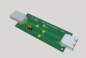
Here is the PCB render:
That's all for now - Langster!


This comment has been removed by a blog administrator.
ReplyDeleteThis comment has been removed by a blog administrator.
ReplyDelete