Showing posts with label FPGA. Show all posts

Sunday, 29 September 2019

More counters with ULX3S and using modules, simulators etc...

Last post covered creating a one second counter in verilog and making an LED flash. In this post I wanted to cover how to make multiple counters. I mentioned in the previous post that multiple counters can be made without a degradation in speed or efficiency and they can be totally independent of each other - bold claims...lets see it done!

Lets make a counter module but unlike before lets make it standalone code that can be used and modified without affecting the inputs and outputs - that way when we need a counter we can just re-use the counter module code and not have to re-write it every time...unless we have a specific requirement to do so.

Here is a simple diagram of what I hope to achieve:


We will have four LEDS changing state depending on the counter output. The clock is our input and the LEDS are the outputs. The part we need to write is the counter module, before we do that though lets think about what we would want in a counter - Lets discuss counter requirements:

Range of the counter - How big a value will we need to count to before we need the count to reset and start again.

Resolution of the counter - What units do we want to count in: Units, Tens, Hundreds, Thousands, Binary???

Count direction - Do we want to count up from a value or count down from a value?

Load - Do we want to be able to start counting from a value other than zero??

Reset - Do we want to be able to reset the count at any time?

Overflow - Do we want to be able to detect if the count reached the maximum value and then started again?

What we are describing here is the behaviour of the counter. This is one way of coding in a hardware description language - The other method is known as structural where the structure of the logic gates needed to realise the function is described.

Before the advent of microcontrollers and FPGA there was (and still is) a very popular integrated circuit that I used called the 74LS163. It was a four bit binary counter with a ripple carry output. That means it could count from zero to fifteen in binary when a positive edged pulse was detected at the CLK pin. Each time an edge is detected the count increased by 1. When the count reached 16 an output was set known as the ripple carry output or RCO. This allowed a designer to cascade the devices together to make a 32 bit counter or a 48 bit counter, or even a 64 bit counter. I'm going to write some verilog code which reproduces the behaviour of the 74LS163 just as an exercise.
The datasheet for a 74LS163 is here just in case people are interested:

74LS163 Datasheet

The inputs for a 74LS163 are:

Here is the verilog code to describe the 74LS163:

// 74LS163 Binary counter module

binary_counter(input a, b, c, d, enp, ent, load, clear, clk,

output qa, qb, qc, qd, rco );

always @(posedge clk)

	begin//start the count on the rising clock edge

	if (!clear)

		begin

			{qd, qc, qb, qa} <=4'b0; //if clear is low, set the count outputs to 0

		end

	if (clear &&!load)

		begin //if load is set low, set count output to match the input

			{qd, qc, qb, qa} <= {d,c,b,a};

		end

	if (clear && load && enp && ent)

		begin//if clear, load, ent and enp are set high, increment the count by one

		{qd, qc, qb, qa} <= {qd, qc, qb, qa} +1;

		end

	end

assign rco = ent ? qa && qb && qc && qd :0; // if the count has reached 15 and ent set high set rco high

endmodule

Lets explain the code:

We have made a module called binary_counter. It has inputs called a, b, c, d, enp, ent, load, clear and clk. It also has outputs called qa, qb, qc, qd and rco. The module section details the inputs and the outputs of the module and their types.

The next section always @(posedge clk) is similar to the main loop in a high level language. This is the description of the circuit that will be free running forever:

When a positive clock edge is detected on the clk input the follwing checks are performed:

Is the clear low? If it is low then set all the outputs to zero.

Is the clear high and the load low? If this is true then set the outputs qa, qb qc and qd to match the inputs a, b, c, d.

Is the clear high, load high enp high and ent high? If this is true then add one to the count value of bits on the outputs qa, qb, qc and qd.

Has the count reached 15 and has there been another clock edge? If this is true set the outputs to zero and set rco high.

If we were to flash this code to the ulx3s it would work...there is a little more code to write before we could use it. It isn't particularly practical though...If we needed a 4 bit binary counter we could just buy one and use it....not recreate it in FPGA fabric...that would be a bit of a waste of resources. The reason I've mentioned it is I want to illustrate the method of describing what is required.

I have found two methods for writing verilog code. The first method is to calculate the logic function required, then draw a diagram of it (structural implementation) and then write verilog code.

The other way is to draw a diagram which describes the behaviour of what is required and then write verilog code. Either method can be applied...I find the latter behavioural method easier.

Going back to our requirements:

Range of the counter - How big a value will we need to count to before we need the count to reset and start again.

It actually doesn't matter. We can decide when to start, stop and reset the count!

Resolution of the counter - What units do we want to count in: Units, Tens, Hundreds, Thousands, Binary???

Again, it doesn't matter. We can decide what increments we use!

Count direction - Do we want to count up from a value or count down from a value?

This time it matters, we can write code which describes both behaviours but we will need an input to set the count direction.

Load - Do we want to be able to start counting from a value other than zero??

This function was useful when using discrete devices with fixed range and resolution. We don't need this anymore as we can have any range and resolution we like.

Reset - Do we want to be able to reset the count at any time?

Yes! We will need an input to be able to start the counter from zero.

Overflow - Do we want to be able to detect if the count reached the maximum value and then started again?

This function was useful when using discrete devices with fixed range and resolution. We don't need this anymore as we can have any range and resolution we like.

Here is a diagram of what our counter would look like:
From this we can write the module statement for our counter:

module up_down_counter(
    input clk,                      // 25 MHz clock input from the top module
	input reset,			  	    // reset input from the top module
	input up_down,				    // count up or down from the top module
    output [24:0] count_output         	// counter output to be passed to top module
);

Next we need an internal signal to act as a register which stores the result of the count process depending on whether the count is up or down, whether the reset is active (high) or a clock edge has been detected...

reg [24:0] count = 0;

Now we need to write the code that describes the actual counting process:

begin
	if(reset)
		count <= 0;
	else if(~up_down)
		count <= count + 1;
	else
		count <= count - 1;
end     

assign count_output = count;

endmodule

Here is the entire code for the module just in case it is needed:

module up_down_counter(
    input clk,                      // 25 MHz clock input from the top module
	input reset,			  	    // reset input from the top module
	input up_down,				    // count up or down from the top module
    output [24:0] count_output         	// counter output to be passed to top module
);
    reg [24:0] count = 0;         // Register for the counter
	
always @(posedge clk or posedge reset)
begin
	if(reset)
		count <= 0;
	else if(~up_down)
		count <= count + 1;
	else
		count <= count - 1;
end     

assign count_output = count;

endmodule

So we have written a module which will count up or down to any value in unit increments...Copy and paste the code into a text file and call it up_down_counter.v

I used this folder:

C:\msys64\src\Alex\ulx3s\Multiple Counters

Now we need to write some code that calls our new counter module and supply the modules with the inputs needed and then couple the outputs to something we can physically see...LEDS!
Before we do that though we should really update our original diagram to reflect the module code we have written because it will help us write our top module.

The up_down counter module looks like this in diagram form:


Now we are going to use this information to update the top level diagram to implement some verilog code which flashes the LEDS at different rates. Here is the diagram:
From the diagram we can now work out what our top module inputs will be:

Clock, Reset, Up / Down

The outputs are LED 0, LED 1, LED 2 and LED 3

From here we are going to write the top.v code which will call the counter module we wrote earlier and attach the inputs and outputs. Before we do that though it is a good idea to simulate the module code to make sure it works as intended.

There are many simulation programs available for verilog. I decided to use the iverilog program which is well documented. The software is written and maintained by Stephen Williams and it is released under the GNU GPL license. I should also mention that I'm using the Windows 10 operating system...

I downloaded it from here: http://bleyer.org/icarus/

I then followed the instructions and read up some tutorials on how to use it. It wasn't too complicated!

I used the instructions from here:

https://www.swarthmore.edu/NatSci/mzucker1/e15_f2014/iverilog.html

Make sure that iverilog is added to your path in Windows! Now we need to write some code which tests the module.

This is known as a test bench and it is some more verilog code:

// Testbench Verilog code for up-down counter
//`timescale 1ns/100ps

`include "up_down_counter.v"  //include the file which contains the module to be tested

// create a test bench module with the inputs and the output(s)
module up_down_counter_testbench(); 
reg clk, reset,up_down;
wire [24:0] count_output;

// instantiate the module to be tested with inputs and output(s)
up_down_counter counter_one
(clk, reset, up_down, count_output);

// tell the simulator what we want the simulation file to be called
// and to get data for all variables
initial begin

	$dumpfile("test.vcd");
	$dumpvars;	
	
end

// monitor the variables so we can see some text output from the simulation
  initial
     $monitor("At time %t, count_output = %h (%0d)",
              $time, count_output, count_output);

// create a clock running for 10 seconds high and 10 seconds low
initial begin 
	clk=0;
	forever #10 clk=~clk;	
end

//exercise the inputs at suitable points in time and finish the simulation

initial begin
	reset=1;
	up_down=0;
	#20;
	reset=0;
	#120;
	up_down=1;
	#500
		
	$finish;
end

endmodule

Create a text file called up_down_counter_tb.v and paste the above code into it. Save the file in the same directory as the other verilog code already written...I used:

C:\msys64\src\Alex\ulx3s\Multiple Counters

The comments for the code should be fairly self explanatory. Now it is time to run the simulation:

Open a command prompt window and navigate to the folder:


Next type the following command:

iverilog -o up_down_counter_tb.vvp up_down_counter_tb.v

The command creates an iverilog simulation file with a vvp extension from our test bench code.
Next type the command:

vvp up_down_counter_tb.vvp

You should see the following output:


A file test.vcd has been created and we can now use this to look at the results of the simulation using a piece of software called GTKWave...

Type the following command:

gtkwave test.vcd

The GTKWave program should load:


Click on the module in the SST box in the top left corner to add the signals:


Double click on each signal to display it's simulated waveform:
Click on the magnifying glass icons to expand the traces to see the output!


Our code works! We can see that while the reset is high no counting occurs. When the reset is low and up_down is low the count increases, when up_down is high the count reduces...

Simulation is a very useful tool to check that the code we have written works as intended...Lets get on with writing the top module code to complete what we set out to do in the first place. It will be quite similar to the test bench code already written.

Create a text file called top.v and save it in the same folder as the other files:

C:\msys64\src\Alex\ulx3s\Multiple Counters

Here comes the code:

module top(
    input clk_25mhz,                // 25 MHz clock input
	output [3:0] led, 				// 4 Bit LED Output register
    output wifi_gpio0			    // Output for Wifi enable	
);
  
  //internal signals
  
  reg [24:0] counter_one_output;    	// Register for the first counter output
  reg reset_counter_one;				// Register for the reset on the first counter
  reg up_down_counter_one=0;			// Register for the up_down on the first counter
  
  reg [24:0] counter_two_output;    	// Register for the second counter output
  reg reset_counter_two;				// Register for the reset on the second counter
  reg up_down_counter_two=0;			// Register for the up_down on the second counter
  
  reg [24:0] counter_three_output;    	// Register for the third counter output
  reg reset_counter_three;				// Register for the reset on the third counter
  reg up_down_counter_three=0;			// Register for the up_down on the third counter
  
  reg [24:0] counter_four_output;    	// Register for the fourth counter output
  reg reset_counter_four;				// Register for the reset on the fourth counter
  reg up_down_counter_four=0;			// Register for the up_down on the fourth counter 

//first counter module instantiation

up_down_counter one_sec_counter(
	.clk(clk_25mhz),
	.reset(reset_counter_one),
	.up_down(up_down_counter_one),
	.count_output(counter_one_output)
);

//second counter module instantiation

up_down_counter half_sec_counter(
	.clk(clk_25mhz),
	.reset(reset_counter_two),
	.up_down(up_down_counter_two),
	.count_output(counter_two_output)
);

//third counter module instantiation

up_down_counter quarter_sec_counter(
	.clk(clk_25mhz),
	.reset(reset_counter_three),
	.up_down(up_down_counter_three),
	.count_output(counter_three_output)
);

//fourth counter module instantiation

up_down_counter eighth_sec_counter(
	.clk(clk_25mhz),
	.reset(reset_counter_four),
	.up_down(up_down_counter_four),
	.count_output(counter_four_output)
);

// initial settings
// resets all high to start counts at same time
// up_down all low to ensure we count up not down

initial begin

reset_counter_one = 1;
reset_counter_two = 1;
reset_counter_three = 1;
reset_counter_four = 1;

up_down_counter_one = 0;
up_down_counter_two = 0;
up_down_counter_three = 0;
up_down_counter_four = 0;

end

always @(posedge clk_25mhz) // react on the positive clock edge

begin
	
	//counter one set to count for one second 
	
	if (counter_one_output == 25000000)    // If the count register has reached 25 million 
                begin
                    led[0] <= ~led[0];      // toggle the LED[0] 
					reset_counter_one = 1;	// set counter one back to zero	
	            end
				
	else reset_counter_one = 0;				// allow counter one to continue
	
	//counter two set to count for 0.5 seconds 
	
	if (counter_two_output == 12500000)    // If the count register has reached 12.5 million 
                begin
                    led[1] <= ~led[1];      // toggle the LED[1] 
					reset_counter_two = 1;	// set counter two back to zero	
	            end
	
	else reset_counter_two = 0;				// allow counter two to continue	
	
	//counter three set to count for 0.25 seconds
	
	if (counter_three_output == 6250000)    // If the count register has reached 6.25 million 
                begin
                    led[2] <= ~led[2];        // toggle the LED[2] 
					reset_counter_three = 1;  // set counter three back to zero		
	            end
	
	else reset_counter_three = 0;			// allow counter three to continue
	
	
	//counter four set to count for 0.125 seconds			
				
	if (counter_four_output == 3125000)    // If the count register has reached 3.125 million 
				begin
                    led[3] <= ~led[3];      // toggle the LED[0] 
					reset_counter_four = 1;	// set counter four back to zero	
	            end
	
	else reset_counter_four = 0;			// allow counter four to continue
	
end

assign wifi_gpio0 = 1'b1; //set the wifi_gpio High
	
endmodule

Copy and paste the above code into top.v and save it in the same directory as before.
Hopefully the code is fairly easy to understand...Here are the critical sections:

module top(

 input clk_25mhz, // 25 MHz clock input
 output [3:0] led, // 4 Bit LED Output register
 output wifi_gpio0// Output for Wifi enable

);

The first part is the module statement with the inputs and the outputs - this module is called top because it is the top module and it has a clock input, an eight bit register called led and a single bit output for the wifi enable.

 //internal signals

 reg [24:0] counter_one_output; // Register for the first counter output

 reg reset_counter_one; // Register for the reset on the first counter

 reg up_down_counter_one=0; // Register for the up_down on the first counter

The above section details the internal signals that are needed to be passed to and from the up_down counter
module:

A 24 bit counter register is needed to take and store the output from the up_down counter module

A reset register is needed to set the reset input inside the up_down counter module

An up_down_counter register is needed to set the up_down input inside the up_down counter module

This is repeated four times as there are four counter modules instantiated. The code for instantiating the module is below:

up_down_counter one_sec_counter(
.clk(clk_25mhz),
.reset(reset_counter_one),
.up_down(up_down_counter_one),
.count_output(counter_one_output)
);

The above code works like this:

Make a counter from the code already written in up_down_counter.v - call it one_sec_counter

connect the clk input inside up_down_counter.v to clk_25mhz (the main clock source on the board)

connect the reset input inside up_down_counter.v to the internal register reset_counter_one

connect the up_down input inside up_down_counter.v to the internal register up_down_counter_one

connect the count_output output inside up_down_counter to the internal register counter_one_output

Because we want the reset and up_down inputs to react at the same time we set them initially:

initial BEGIN reset_counter_one = 1; reset_counter_two = 1; reset_counter_three = 1; reset_counter_four = 1; up_down_counter_one = 0; up_down_counter_two = 0; up_down_counter_three = 0; up_down_counter_four = 0; END

Finally we have the code which makes the FPGA react when the counters have reached a defined count:

always @(posedge clk_25mhz) // react on the positive clock edge

begin

//counter one set to count for one second

if (counter_one_output == 25000000) // If the count register has reached 25 million

 begin

 led[0] <= ~led[0]; // toggle the LED[0]

 reset_counter_one = 1; // set counter one back to zero

 end

else reset_counter_one = 0; // allow counter one to continue

When counter one has reached twenty-five million (one second) toggle led[0] to its alternative state, reset the count

If counter one hasn't reached twenty-five million don't reset the count...
Why twenty-five million? Well....25 MHz is the external clock frequency...that means the external clock oscillates twenty-five million times per second so if we want a count every second we need to count twenty-five million clock edges...

Lets upload the code to the board -  fire up ConEmu.exe (Windows) and navigate to the folder:

C:\msys64\src\Alex\ulx3s\Multiple Counters

Remember that the board I'm working with has an ECP5 45F Lattice Semiconductor FPGA so the commands are tailored to it. If you are working with a ECP5 12F board or an ECP5 85F board you will need to change to commands appropriately:

Type the following command into the console:

apio build --board ulx3s-45f


Ignore the warnings ;)

Make sure you have the ULX3S development board connected via USB!

Now lets upload the bitstream to the ULX3S development board:

apio upload --board ulx3s-45f


Finally clean up the directory:

apio clean


If all went according to plan you should see the leds on the ULX3S board flashing!


Well...that was a lot of work! Apologies for the really long post. There was a lot to get through! Next post will be something simple and more fun hopefully!

Cheers for now - Langster!

Sunday, 8 September 2019

Counters in Verilog with the ULX3S

It's time for another learning experience with the ULX3S.  When using FPGAS or Microcontrollers in general it's very useful to generate and use counters.  Counters as their name suggest are ways time can be added to logic circuits.  If you wanted an LED to flash once a second use a counter.  If you want several LEDS to flash at different rates independently use several counters...If you want to ensure an event occurs at a specific point in time...use a counter.

Counters in FPGA are particularly cool as you can have as many of them as you like or need, unlike microcontrollers.  The other thing is that the counters are all independent of each other in an FPGA.  So multiple counters can be used to control things without affecting the operating of anything else...that's very hard to achieve with a microcontroller...the program flow is always linear.

Lets make a counter flash an LED once a second. In order to do that we need to know a couple of things:

What is the clock speed of the oscillator used on the ULX3S development board?
What is the control logic for the LEDS (active high or active low)?

We can find these answers either from the schematic of the ULX3S or from the constraints file.  Both of which are helpfully available here:

https://github.com/emard/ulx3s

https://github.com/emard/ulx3s-examples/blob/master/README.md

The schematic is broken down into several pages and was created in KiCad.  There is also a PDF version here:

https://github.com/emard/ulx3s/blob/master/doc/schematics.pdf

We are interested in page 4 called 'Blinkey' and page 6 called 'USB'.  Blinkey shows the eight LEDS referenced from zero to seven in the centre of the page four in cell B,3.  The LEDS are common ground connected which means they are 'active high' - A control signal from 'Bank 7' the FPGA needs to be high in order to get an LED to turn on.  The current limiting resistors used are 549 ohms so with 3.3 Vdc logic the current flowing through each LED when on will be 6 mA - bright enough! I've used FPGA development boards in the past where the IO was active low so its useful information to know.


The oscillator is in cell A, 3 on the top middle of the page and it is referenced as being 25 MHz - also useful to know.  It is of course possible to use phase lock loops to generate faster clock signals if that is what is required.


The User Constraints File or UCF as it is sometimes referred to is a list of information which tells the software which pins on the FPGA are connected to what and more usefully how they are referred to.  We could write our own UCF file if we wanted to and for complicated designs or if we had created our own circuit with an FPGA we would have to write our own. Helpfully the board designer of the ulx3s (EMARD) has written one for us. When we come to write the verilog code we can use the same naming convention and that way we don't have to write our own UCF file.

The sections we are interested in are:

# The clock "usb" and "gpdi" sheet
LOCATE COMP "clk_25mhz" SITE "G2";
IOBUF  PORT "clk_25mhz" PULLMODE=NONE IO_TYPE=LVCMOS33;
FREQUENCY PORT "clk_25mhz" 25 MHZ;

and

## LED indicators "blinkey" and "gpio" sheet
LOCATE COMP "led[7]" SITE "H3";
LOCATE COMP "led[6]" SITE "E1";
LOCATE COMP "led[5]" SITE "E2";
LOCATE COMP "led[4]" SITE "D1";
LOCATE COMP "led[3]" SITE "D2";
LOCATE COMP "led[2]" SITE "C1";
LOCATE COMP "led[1]" SITE "C2";
LOCATE COMP "led[0]" SITE "B2";
IOBUF  PORT "led[0]" PULLMODE=NONE IO_TYPE=LVCMOS33 DRIVE=4;
IOBUF  PORT "led[1]" PULLMODE=NONE IO_TYPE=LVCMOS33 DRIVE=4;
IOBUF  PORT "led[2]" PULLMODE=NONE IO_TYPE=LVCMOS33 DRIVE=4;
IOBUF  PORT "led[3]" PULLMODE=NONE IO_TYPE=LVCMOS33 DRIVE=4;
IOBUF  PORT "led[4]" PULLMODE=NONE IO_TYPE=LVCMOS33 DRIVE=4;
IOBUF  PORT "led[5]" PULLMODE=NONE IO_TYPE=LVCMOS33 DRIVE=4;
IOBUF  PORT "led[6]" PULLMODE=NONE IO_TYPE=LVCMOS33 DRIVE=4;
IOBUF  PORT "led[7]" PULLMODE=NONE IO_TYPE=LVCMOS33 DRIVE=4;

Just for reference a hash ( '#' ) symbol before a line means that the text after that is a comment

LOCATE COMP means to locate the drive logic to a particular section within the FPGA fabric.
IOBUF  PORT means the line is to be configured as a buffered input or output..
PULLMODE=NONE means the line will not have an internal pull up or pull down resistor enabled.
IO_TYPE=LVCMOS33 means the line will be configured to be low voltage CMOS at 3.3 Vdc.
DRIVE=4 means the line will be able to source 16 mA of current.  Drive 1 = 4 mA, Drive 2 = 8 mA, Drive 3 = 12 mA and finally drive 4 - 16 mA

When we write the verilog code we need to refer to the clock as clk_25mhz and the individual leds as led[0]

I was really hoping to use a program called IceStudio to program the ulx3s as it is essentially a graphical front end for apio which collates the usage of Yosys, Ptrellis and NextPNR.  Unfortunately the developers of IceStudio do not wish to add the ulx3s to the list of supported development boards.  They have their reasons for doing that.  I suspect it would be possible to fork IceStudio to work with ULX3S but I'm not going to do that as:
  1. I don't have the skill!
  2. I don't have the time to learn the skill!
  3. I don't want to annoy the IceStudio developers because they are nice guys and have worked hard.
I can use the program to demonstrate what we are going to do though...very useful. I find graphical information easier to pick up over seeing lines of HDL Syntax.


The diagram is meant to show that we have one input called clk_25mhz, we have two outputs called LED and wifi_gpio.

The blue box labelled PrescalerN is some pre-written code which basically is a verilog counter module.  It will take the clock input, count how many clock pulses there are and when it has reached 25 000 000 counts it will send a signal to the LED output.  The wifi_gpio output will be set high.

In verilog code this looks like this:

module top (
    input clk_25mhz,            // 25 MHz clock input 
    output reg led [7:0] = 1'b0,   // 8 Bit LED Output register, set LED[0] to be in a predefined state
    output wifi_gpio0     // Output for Wifi enable 
);
    reg [24:0] count = 0;          // Register for the counter
 
    always @(posedge clk_25mhz)    // Interrupt at the positive 25 MHz clock edge
    begin
       if (count == 25000000)    // If the count register has reached 25 million
                begin
                    led0 <= ~led0; // toggle the LED[0] On and OFF with a one second interval.
                    count <= 1'b0; // and reset the count to 1 (binary) 
                end
            else                   // else
                begin    
                    count <= count + 1'd1; // increment the count by 1
                end
    end

    assign wifi_gpio0 = 1'b1; //set the wifi_gpio High

endmodule

The code should be fairly easy to follow. The wifi_gpio input is only needed if your board has an ESP32. The command enables the ESP32 so code can be pushed over wifi. I haven't been doing that at the moment although I should! I'm fairly certain the code will work, I would like to have tested it and in later posts I will be looking into open source verification software like verilator and GTKwave. These programs allow one to simulate verilog code and show how the inputs and outputs will respond.

Lets save the text file (call it top.v) somewhere sensible I chose: C:\msys64\src\Alex\ulx3s\One Second Counter

 Next copy in the constraints file and apio.ini and fire up ConEmu.exe (Windows) and navigate to the folder we just made. It's also at this point that I should state that the board I'm working with has an ECP5 Lattice Semiconductor FPGA so the commands are tailored to it. If you are working with a ECP 12F board or an ECP 85F board you will need to change to commands appropriately.


Type the following command to turn the verilog code in top.v into the bit file ready for uploading to
the ulx3s development board: 

apio build --board ulx3s-45f 

The output should look like this:
 
Ignore the warnings... Plug in the ulx3s into your computer using a microUSB cable - exciting times! 

Next lets upload to the ulx3s development board: 

apio upload --board ulx3s-45f 

The output should look like this:
 

Finally its good practice to remove unnecessary files from the build process: 

 apio clean 

 As everything worked you should be able to see an LED flash like in the video below: 


Again not the most exciting thing in the world but it is the hello world of FPGAS and from a tiny acorn an mighty oak tree grows ;) 

That is all for now - Langster!

Thursday, 5 September 2019

ULX3S Open Source FPGA Development Board

I have made no secret of the fact that I am interested in FPGA technology and have been trying to relearn VHDL for some time.  I am also very keen on using open source programs and development tools.

Recently (sometime in the last couple of years) I heard about project IceStorm by Clifford Wolfe.  Mr Wolfe has reverse engineered Lattice Semiconductor's bit-stream files and written a software tool called Yosys which is used to convert verilog files into mapping files which can then be loaded onto a lattice semi-conductor FPGA.  At the moment proprietary FPGA development tools are very large pieces of software which take a lot of space on a hard disk, are feature heavy and not free to use (require licence files), often unsupported (Xilinx WEBise anyone) and I found difficult to use.  I'm not saying they aren't good but if I can use open source software tools I will...I like the idea behind the licensing models.  I'll donate what I can afford and assist wherever I can.

The Yosys Website is here: http://www.clifford.at/yosys/

Project ICE Storm: http://www.clifford.at/icestorm/

Until recently I didn't have a Lattice Semiconductor FPGA development board but that changed when I was offered a ULX3S open source board from the very clever guys at the Radiona Hackspace.  I had come into contact with these gentlemen when I was trying to learn to use the Elbert V2 and Mimas V2 Xilinx based FPGA development boards.  They developed a very cool piece of kit to make use of the open source tools for teaching a Digital Logic course at their local university.

The ULX3S with 3D printed case and buttons!
The board arrived in very good order with a 3D printed case, buttons and some pre-built examples.  I had a quick play with it and intended to write up my experiences and get started on using it.  That was probably this time last year...I am attempting to get back into blogging my experiences, trials and tribulations outside of work as I find it quite useful and I find it forces me to improve on my electronics and development skills.  Anyway...back to the board:

The board is in my opinion, very well designed and implemented.  I particularly like the addition of the ESP32 so files can be uploaded over wifi.

Here are some photos of the board:

The top side of the PCB with buttons, microSD card and display
The underside of the PCB with the ESP32 module
Here is the website for the project: https://radiona.org/ulx3s/

Here is a Hackaday write up: https://hackaday.com/2019/01/14/ulx3s-an-open-source-lattice-ecp5-fpga-pcb/#more-340565

I'll be honest, I bought the board to support the project, I haven't got a project or use in mind.  To be even more honest I still want to re-learn a hardware description language so that when I do have a project in mind I'll be able to make use of the technology.  I do have ideas for a piece of instrumentation but that is a way off and requires a lot more than just the FPGA!

The first thing I did with the board was use it to emulate an Amiga 500 computer using the pre-loaded Minimig project which came ready to play on the board.  All I had to do was grab some amiga disk images and I could play all the games from my misspent youth.  Retro gaming with FPGA devices is a very popular hobby as the hardware is not being emulated but actually realised within the fabric of the device which leads to a more realistic experience.

Playing Lotus Turbo Challenge 2 and Utopia are fun diversions but not quite what I had in mind for the device.

The open source tools all appear to be for linux operating systems only at the moment so I installed Linux Mint on my main PC and got to work installing all of the pieces of software needed from project Ice storm.  

My LinuxFu is not that strong so I may have messed this up somewhere along the way.  I know I have downloaded, and compiled the following pieces of software:

IceStudio
prjtrellis
Yosys
nextPNR

I was then pointed towards the apio project by a colleague and downloaded the windows version of that software along with all the other bits and pieces needed by following the instructions here:

https://github.com/ulx3s/fpga-odysseus

It installed fine although I would ensure that if following the instructions that you don't upgrade the apio software.

Once presented with the command prompt by loading the ConEmu.exe program it is pretty easy to get started:


This screen brought my back to my days of the DOS prompt.  I know the linux command prompt is fairly similar but I just don't use linux enough to be comfortable with it...I am slowly improving though...

I made a folder called Alex and then a sub folder called ulx3s, you could use any folder names you like.  I then copied two files into the folder:

apio.ini - found from the folder C:\msys64\src\fpga-odysseus\tutorials\01-Basics\01-LED
ulx3s_v20.lpf - found from the folder C:\msys64\src\fpga-odysseus\tutorials\01-Basics\01-LED

The apio.ini file is a text file that tells the apio software everything needed to prepare files for upload to the ulx3s board and ulx3s_v20.lpf is the constraints file for the board, it tells apio and all of the other software which pins are connected to what and where between the FPGA and the external peripherals.

I next created a simple text file in notepad++ - you could use any text editor to be honest.  I called it top.v and typed out the following simple program:

//Hello world LED program

//create a module called top
module top (
    output [7:0] led, //create an output vector called 'led' with 8 bits
    output wifi_gpio0 //create an output for the wifi gpio
);
    assign led = 8'b10101010; //set the state of the bits in the vector to the number 170
 // this sets the bits on and off alternately

    assign wifi_gpio0 = 1'b1; // set the wifi gpio wifi high 
endmodule //end the module

Save the file in the directory made previously:

C:\msys64\src\Alex\ulx3s

Next jump to the ConEmu command prompt and make sure all of the files we need are there by typing ls and hit enter :


next type the following: apio build --board ulx3s-45f'

You should see the following displayed, ignore the warning messages:


  The following files will have been created in the directory:

Exciting times....now it is time to upload the program to the FPGA.  Make sure the ULX3S board is plugged into a suitable USB port and powered up.

Type the following command:

apio upload --board ulx3s-45f

If all goes according to plan you should see the following:


Next type the following:

apio clean

This removes all of the unnecessary files created during the processes.  Finally its time to admire your work.  If everything went according to plan you should see the following LED pattern on your ULX3S!


Ok so its nothing special but it's a start. I'm hoping soon to do a bit more with it.  I hear good things about something called ICE Studio:

https://icestudio.io/

It doesn't have support for the ulx3s yet but I'm hopeful it can be added soon!

That's all for now - Langster!

Tuesday, 12 September 2017

Using Components in VHDL

Recently I was asked to provide a bit of assistance with some VHDL code - One of the blog readers was looking to implement a logic based CPU on the Mimas V2 Development board. I don't claim to be an expert in VHDL but the crux of his issue was using pre-written code in one project several times. The beauty of FPGA technology is that as long as there is space within the device and pins available it is possible to have as many logic functions as one wants!

There comes a point in FPGA programming where trying to put all of the code in one single source file becomes really awkward. The file would become very long to read and debug and it may make more sense to take a modular approach and re-use code from previous designs. Luckily for the FPGA design engineer it is possible to write and design modules in VHDL very easily and each module can be tested and used on it's own.

The way to implement this is to use the component keyword in VHDL and 'instantiate' as many of the modules or blocks of code as one wants.

In previous posts I have already used this method but I haven't really ever discussed it explicitly so here goes:
In a VHDL source module the code is organised into section statements known as:
  • Entities - The statement which defines the external input and output connections of the module.
  • Architectures - This is the code section which actually tells or defines the function of the module.
  • Components - A statement within the architecture section which allows the designer to link internal signals or external signals with pre-written VHDL code in another module.
  • Instances - A statement which actually creates the 'instance' of the external module code within another module. A designer can have multiple instances of a module within a design with one component statement as long as all of the connections are correctly port mapped.
Here is an example of an Entity statement:

entity EntitySection is
           Port ( clkinput : in STD_LOGIC;
                  input1 : in STD_LOGIC;
                  input2 : in STD_LOGIC;
                  input3 : in STD_LOGIC;
                  output1 : out STD_LOGIC;
                  output2 : out STD_LOGIC);
end EntitySection;

You can have as many inputs and outputs as you like and there can be combined inputs and outputs. The green text are keywords and cannot be used as labels. The red text are labels which are used to remind the designer what the entity's purpose is. The black text are the defined inputs and outputs. The blue text are the type of inputs and outputs.

Here is an example of an Architecture statement:

architecture Behavioral of EntitySection is 
begin 
      input1 <= not input2; 
end Behavioral;

This is the section of code that defines how the internal signals and external signals will interact to realise the function required. As before the green text are keywords, the red text are labels and the black text are the inputs and outputs.

Here is an example of a Component statement:

COMPONENT Not_gate 
          PORT( input1  : IN std_logic
                output1 : OUT std_logic); 
END COMPONENT;

As above, the different colours relate to keywords, labels, definitions and types.
Here is an example of a Instantiation statement:

Inst_Not_gate: Not_gate 
         PORT MAP(
                   input1  => input_signal1, 
                   output1 => output_signal1 
                  );

The instantiation code is the way the designer defines how the signals from the component module connect to the signals within the source module. These signals in the source module could be internal or external signals.

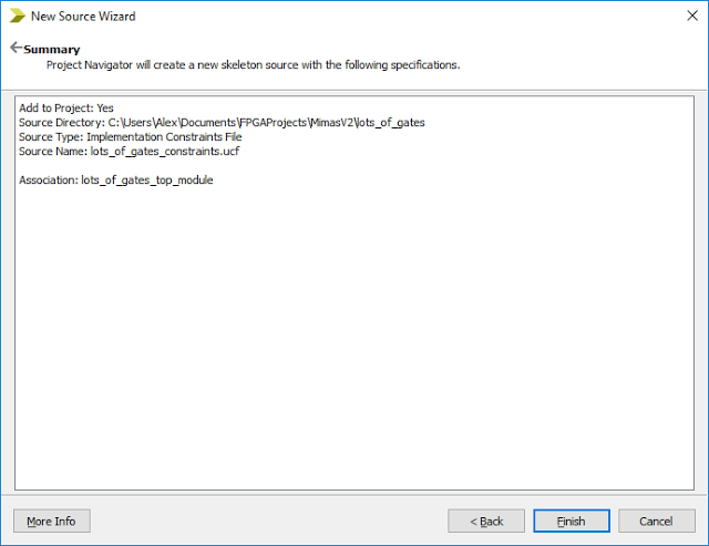
As an example lets write some simple two input logic gates in VHDL code and then'instantiate multiple versions of them in VHDL and then simulate their function and then finally show the results working on the Mimas V2 FPGA Development board. In theory any FPGA development board could be made to work including the Elbert V2 (I will share the Elbert V2 version also as I know some people are using those boards).

Load up Xilinx WebISE and start a new project - I called mine Lots of gates and placed it in a suitable folder on the hard disk.


Click next when ready to continue...


Input the settings shown (These are correct for the Numato Labs Mimas V2 development board).
Then click next when ready...


Click Finish to return to the main project screen within Xilinx WebISE:


Next right click on the Hierarchy window and select Add new source:


Select VHDL source module and give it a suitable name - I called mine Not_gate:


Click Next when ready to continue and enter the inputs and outputs for the Not_gate module. I chose to have an input and an output - to create a single inverter.


Click Next when ready to continue and display the summary page:


Click Finish to return to the main project window:


The WebISE software has helpfully created some code for us based on the decisions we made. I like to delete the comments (green text) as I don't find them helpful:


Now we need to write the architecture statement to make the module behave as an inverter or Not gate. It is very simple as the inverter function is already present within VHDL. Here is the code for the entire module:

library IEEE
use IEEE.STD_LOGIC_1164.ALL

entity Not_gate is 
    Port ( A : in STD_LOGIC
           B : out STD_LOGIC); 
    end Not_gate

architecture Behavioral of Not_gate is 
  begin 
     B <= not A; 
  end Behavioral;

Now save the module - just in case...and then right click on the synthesize – XST process and select run. The software checks the code written is correct. Once the process has completed there will be a green tick on that section:


Now let’s simulate the code we have just written to ensure it works properly before we use it. It's always a good idea to simulate things to make sure that it works as intended.

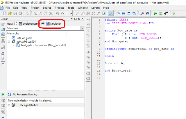
Click on the simulate radio button on the Hierarchy window:


Next right click on the Hierarchy window and select Add new source:


Select VHDL test bench and call the file something sensible...I called mine Not_gate_tb. Click Next when ready to continue:


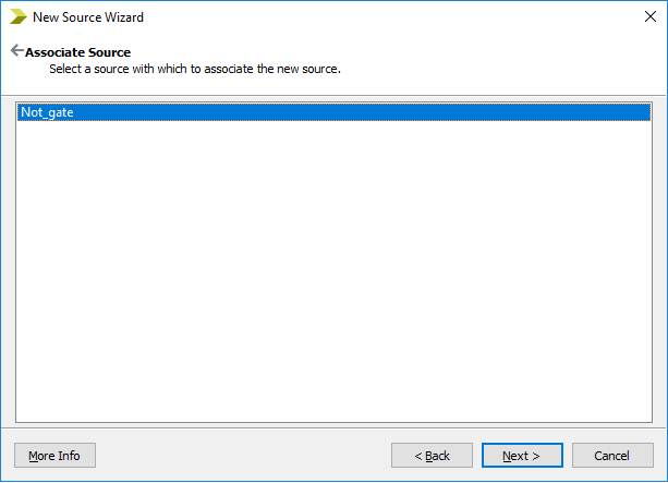
Associate the test bench source file with the code you wish to simulate...click Next when ready to continue:


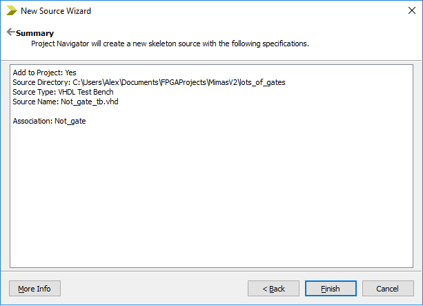
Click finish to continue and return to the main project window:


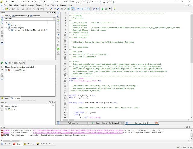
Helpfully Xilinx WebISE has automatically generated the test bench code for us...unhelpfully it has also introduced some errors. Don't worry about these for now...the code generated is expecting a clock source to be present. There isn't a clock source in our design as we did not need one. We will remove the errors when we modify the test bench code. Again I like remove the top comments as I don't need them. Comments are useful but only when necessary...

Here is the code with the comments removed:

LIBRARY ieee;
USE ieee.std_logic_1164.ALL;
 
ENTITY Not_gate_tb IS
END Not_gate_tb;
 
ARCHITECTURE behavior OF Not_gate_tb IS 
 
    -- Component Declaration for the Unit Under Test (UUT)
 
    COMPONENT Not_gate
    PORT(
         A : IN  std_logic;
         B : OUT  std_logic
        );
    END COMPONENT;
    

   --Inputs
   signal A : std_logic := '0';

  --Outputs
   signal B : std_logic;
   -- No clocks detected in port list. Replace <clock> below with 
   -- appropriate port name 
 
   constant <clock>_period : time := 10 ns;
 
BEGIN
 
 -- Instantiate the Unit Under Test (UUT)
   uut: Not_gate PORT MAP (
          A => A,
          B => B
        );

   -- Clock process definitions
   <clock>_process :process
   begin
  <clock> <= '0';
  wait for <clock>_period/2;
  <clock> <= '1';
  wait for <clock>_period/2;
   end process;
 

   -- Stimulus process
   stim_proc: process
   begin  
      -- hold reset state for 100 ns.
      wait for 100 ns; 

      wait for <clock>_period*10;

      -- insert stimulus here 

      wait;
   end process;
 
END;

Now we need to remove the code relating to the automatically generated clock as this isn't
required:

LIBRARY ieee;
USE ieee.std_logic_1164.ALL;
 
ENTITY Not_gate_tb IS
END Not_gate_tb;
 
ARCHITECTURE behavior OF Not_gate_tb IS 
 
    -- Component Declaration for the Unit Under Test (UUT)
 
    COMPONENT Not_gate
    PORT(
         A : IN  std_logic;
         B : OUT  std_logic
        );
    END COMPONENT;
    

   --Inputs
   signal A : std_logic := '0';

  --Outputs
   signal B : std_logic;
 
BEGIN
 
 -- Instantiate the Unit Under Test (UUT)
   uut: Not_gate PORT MAP (
          A => A,
          B => B
        );

   -- Stimulus process
   stim_proc: process
   begin  
      -- hold reset state for 100 ns.
      wait for 100 ns; 

      -- insert stimulus here 

      wait;
   end process;

END;

The code generated actually uses the component statement so our automatically generated code is a perfect example of how a statement should be used! In the architecture statement we can see the component declaration for the Not_gate. Below that section some internal signals are defined to connect to the component we would like to simulate. Underneath that section we have the instantiation section which creates a version of the not_gate called 'uut' and maps the internal signal connections to the component signal connections. Now we need to write some code in the stimulus process section which sets the A input signal to a known value so that the simulator can run the code in the Not_gate module and display what will happen at the output signal - B.

As the module is an inverter or not gate it should be obvious that whatever logic level is present at the output signal is the opposite or inverse of the input signal. For more complicated modules this might be more difficult to assess which is why simulation is useful. It is also possible to see if there are any timing or sequencing issues present with more complicated modules. Simulation can be a very useful diagnostic tool when developing FPGA code.

Let’s write the stimulus VHDL code to test the module code and provide the simulator some information. Let’s set the 'A' input of the inverter to logic '1' for 100 ns and then set it to logic '0' for 100 ns and then set it to an unknown logic level 'X' for 100 ns. When we run the simulator we will be able to visually see what the output signal 'B' does when presented with those input 'stimuli' or logic states.

*Stimuli - a latin word which is the plural of stimulus, to provide a specific functional reaction!

Here is the code:

-- Stimulus process
   stim_proc: process
   begin  
      -- hold reset state for 100 ns.
      wait for 100 ns; 

      A <= '1';
  wait for 100 ns; 
  
  A <= '0';
  wait for 100 ns;
  
  A <= 'X';
  wait for 100 ns;

      wait;
   end process;

Let’s save the code and run the simulator! Click on the Not_gate VHDL test bench module in the Hierarchy window:


Next right click on 'Behavioral Check Syntax' in the process window and select Run:


Once the process has completed there should be a green tick present:


Next right click on Simulate Behavioral Model and select Run:


Once the process has completed the ISIM screen will be displayed showing the results of the simulation:


At first it looks as though the simulation has failed as the result traces are red and in an X state - don't worry though that is what was expected. The last state we simulated was an 'X' state for the input signal. Click on the 'Zoom to Full View' icon on the toolbar to display the full results traces:


The green part of the traces show how the input 'A' went from a logic '0' to a logic '1' after 100 ns and the output 'B' changed accordingly. Then the input 'A' went from a logic '1' to a logic '0' for 100 ns and then the input 'A' was set to an unknown logic state 'X' and the output 'B' responded with a logic 'X' for the rest of the simulation - exactly what the test bench code was meant to do. So our simulation worked perfectly and more importantly the Not_gate module works perfectly!

This module can now be reused as many times as we like in any of our designs - Most Excellent!

Close down the ISIM application as we are finished with that program to return to the main project screen.

Let’s add some more logic functions like the AND, OR, and XOR functions. I'm not going to show all of the steps with pictures this time though, it's the same process as before.

Click on the implementation radio button and then add new VHDL source modules to the project. I called mine And_gate, Or_gate and XOR_gate. I chose to make them all two input devices with one output.


Here is the project window with all of the VHDL source file modules:


I deleted all of the comments that were not needed for each of the new modules and added the necessary code for the architecture sections. The code should be pretty self-explanatory but just in case here is the VHDL code for each logic function:

And Gate logic function VHDL code:

library IEEE;
use IEEE.STD_LOGIC_1164.ALL;

entity And_Gate is
    Port ( A : in  STD_LOGIC;
           B : in  STD_LOGIC;
           Q : out  STD_LOGIC);
end And_Gate;

architecture Behavioral of And_Gate is

begin

   Q <= A and B;

end Behavioral;

Or Gate logic function VHDL code:

library IEEE;
use IEEE.STD_LOGIC_1164.ALL;

entity Or_gate is
    Port ( A : in  STD_LOGIC;
           B : in  STD_LOGIC;
           Q : out  STD_LOGIC);
end Or_gate;

architecture Behavioral of Or_gate is

begin

Q <= A or B;

end Behavioral;

Xor Gate logic function VHDL code:

library IEEE;
use IEEE.STD_LOGIC_1164.ALL;

entity Xor_gate is
    Port ( A : in  STD_LOGIC;
           B : in  STD_LOGIC;
           Q : out  STD_LOGIC);
end Xor_gate;

architecture Behavioral of Xor_gate is

begin

Q <= A xor B;

end Behavioral;

Ensure each VHDL module has the correct code. If you were so inclined you could then simulate each module to make certain the code behaves as intended. I'm not going to bother this time but for more complicated modules it's very important that it's simulated. I have saved myself hours of debugging by simulating the module behaviour before continuing.

At this point I like to draw a diagram which shows what function I want all of these modules to perform when connected together. Normally I would do this before I start writing the code but as this is just an example I'm doing it now. Lets implement each logic gate into the FPGA and use the DIP switches to connect to the inputs of the logic gates and then lets connect the outputs of the logic gates to the LEDS so that we can see the results when we change the state of the DIP switches!


From the diagram we can now create a VHDL top module which will connect to the DIP switches and LED and we can then make components to call all of the other modules and connect those modules inputs and outputs to the top module's inputs and outputs. Sounds complicated but it is actually fairly simple. Lets create the top module by right clicking in the hierarchy window as before...I called mine lots_of_gates_top_module:


Click Next and lets select how many inputs and outputs we will need. We need one input and output for the Not gate, two inputs and one output for the And gate, Or gate and Xor gate. So that makes seven inputs and four outputs. Give the inputs and outputs sensible names:


Click next to display the summary screen:


Click Finish to return to the main project screen.


Again remove the comments that are not necessary. Add comments later if required...


Now we need to add the component statements in the architecture section. The first
component we want to add is the Not gate. There is a really cool and easy way to do this thanks to Xilinx WebISE all we have to do is click on the module we want to use and then click on the Design Utilities option in the process window and double click on 'View HDL Instantiation Template':


We can then select and copy the code without the comments and paste it into the architecture section of the top module. It saves typing and it's completely correct! All we then need to do is correctly complete the port map section and our first component is done:


The Not_gate component signal connections map to the Not_input signal and the Not_Output_LED signal. I also changed the component instantiation label to something more meaningful. It can get awkward when you have multiple components of the same type if you don't use a sensible naming convention:


Repeat the process for all of the other components we intend to add. Once you have done that we need to move the instantiation sections to the begin and end section of the architecture statement. Once complete the code should look like this:


library IEEE;
use IEEE.STD_LOGIC_1164.ALL;

entity lots_of_gates_top_module is
    Port ( Not_input : in  STD_LOGIC;
           Not_Output_LED : out  STD_LOGIC;
          
     And_A_Input : in  STD_LOGIC;
           And_B_Input : in  STD_LOGIC;
           And_Q_Output_LED : out  STD_LOGIC;
          
     Or_A_Input : in  STD_LOGIC;
           Or_B_Input : in  STD_LOGIC;
           Or_Q_Output_LED : out  STD_LOGIC;
          
     Xor_A_Input : in  STD_LOGIC;
           Xor_B_Input : in  STD_LOGIC;
           Xor_Q_Output_LED : out  STD_LOGIC);
end lots_of_gates_top_module;

architecture Behavioral of lots_of_gates_top_module is

 COMPONENT Not_gate
 PORT(
  A : IN std_logic;         
  B : OUT std_logic
  );
 END COMPONENT;

 COMPONENT And_Gate
 PORT(
  A : IN std_logic;
  B : IN std_logic;         
  Q : OUT std_logic
  );
 END COMPONENT;

 COMPONENT Or_gate
 PORT(
  A : IN std_logic;
  B : IN std_logic;         
  Q : OUT std_logic
  );
 END COMPONENT;

 COMPONENT Xor_gate
 PORT(
  A : IN std_logic;
  B : IN std_logic;         
  Q : OUT std_logic
  );
 END COMPONENT;

begin

 Not_gate_1: Not_gate PORT MAP(
  A => Not_input,
  B => Not_Output_LED
 );

 And_Gate_1: And_Gate PORT MAP(
  A => And_A_Input,
  B => And_B_Input,
  Q => And_Q_Output_LED
 );

 Or_gate_1: Or_gate PORT MAP(
  A => Or_A_Input,
  B => Or_B_Input,
  Q => Or_Q_Output_LED
 );

 Xor_gate_1: Xor_gate PORT MAP(
  A => Xor_A_Input,
  B => Xor_B_Input,
  Q => Xor_Q_Output_LED
 );

end Behavioral; 

The code should be fairly self-explanatory. Save the module and now let’s simulate it to make sure it will work as intended. Using the same process as before let’s create a test bench forthe top module and make sure that everything will work.

Click on the simulate radio button in the hierarchy window and then add a new source, select VHDL test bench and give it a suitable name. I called mine lots_gates_test_bench. Then associate the module with the lots_of_gates VHDL module and click finish. Then WebISE will generate some code for us. Delete the comments as necessary. After that delete the clock sections as we don't need those sections.

Finally all that is needed is to write the stimuli section like before. Lets exercise each gate in turn with suitable logic levels and allow time for each state to be easily viewed on the simulator screen. We could exercise all the gates at once but I prefer to see each state separately.

Here is the stimulus code:

library IEEE;
use IEEE.STD_LOGIC_1164.ALL;

entity lots_of_gates_top_module is
    Port ( Not_input : in  STD_LOGIC;
           Not_Output_LED : out  STD_LOGIC;
          
     And_A_Input : in  STD_LOGIC;
           And_B_Input : in  STD_LOGIC;
           And_Q_Output_LED : out  STD_LOGIC;
          
     Or_A_Input : in  STD_LOGIC;
           Or_B_Input : in  STD_LOGIC;
           Or_Q_Output_LED : out  STD_LOGIC;
          
     Xor_A_Input : in  STD_LOGIC;
           Xor_B_Input : in  STD_LOGIC;
           Xor_Q_Output_LED : out  STD_LOGIC);
end lots_of_gates_top_module;

architecture Behavioral of lots_of_gates_top_module is

 COMPONENT Not_gate
 PORT(
  A : IN std_logic;         
  B : OUT std_logic
  );
 END COMPONENT;

 COMPONENT And_Gate
 PORT(
  A : IN std_logic;
  B : IN std_logic;         
  Q : OUT std_logic
  );
 END COMPONENT;

 COMPONENT Or_gate
 PORT(
  A : IN std_logic;
  B : IN std_logic;         
  Q : OUT std_logic
  );
 END COMPONENT;

 COMPONENT Xor_gate
 PORT(
  A : IN std_logic;
  B : IN std_logic;         
  Q : OUT std_logic
  );
 END COMPONENT;

begin

 Not_gate_1: Not_gate PORT MAP(
  A => Not_input,
  B => Not_Output_LED
 );

 And_Gate_1: And_Gate PORT MAP(
  A => And_A_Input,
  B => And_B_Input,
  Q => And_Q_Output_LED
 );

 Or_gate_1: Or_gate PORT MAP(
  A => Or_A_Input,
  B => Or_B_Input,
  Q => Or_Q_Output_LED
 );

 Xor_gate_1: Xor_gate PORT MAP(
  A => Xor_A_Input,
  B => Xor_B_Input,
  Q => Xor_Q_Output_LED
 );

end Behavioral; 

Let’s check the syntax and run the simulator!

Here is the result, I did manipulate the traces to put the outputs next to the inputs:


Close down the simulator...It’s time for the final bit of code writing - creating the implementation constraints file to tell WebISE how the external devices will connect to the FPGA signals in our design. In the hierarchy window click on add new source and choose implementation constraints file:


Click next to continue:


Click Finish to return to the main project screen. Now we need to decide how we want our DIP switches and LEDS to connect to our inputs and outputs.
  • Let’s set DIP switch 0 to be the Not gate input
  • Let’s set LED 0 to be the Not gate output
  • Let’s set DIP switch 1 to be the AND gate A input
  • Let’s set DIP switch 2 to be the AND gate B input
  • Let’s set LED 1 to be the AND gate Output
  • Let’s set DIP switch 3 to be the OR gate A input
  • Let’s set DIP switch 4 to be the OR gate B input
  • Let’s set LED 3 to be the OR gate Output
  • Let’s set DIP switch 5 to be the XOR gate A input
  • Let’s set DIP switch 6 to be the XOR gate B input
  • Let’s set LED 5 to be the XOR gate Output
It is possible to use the WebISE software to generate the constraints for us but I prefer to write my own code using the supplied constraints file from Numato Labs as a template.

Here is the code:

#++++++++++++++++++++++++++++++++++++++++++++++++++++++++++++++++++#
# This file is a .ucf for Mimas V2                                 #
# To use it in your project :                                      #
# * Remove or comment the lines corresponding to unused pins in    #
# the 
project                                                      #

# * Rename the used signals according to the your project          #
#++++++++++++++++++++++++++++++++++++++++++++++++++++++++++++++++++#

CONFIG VCCAUX = "3.3" ;
#NET "CLK" LOC = V10 | IOSTANDARD = LVCMOS33 | PERIOD = 100MHz;
#NET "RST_n" IOSTANDARD = LVCMOS33 | PULLUP;

#################################################################################
# DIP Switches                                                                  #
#################################################################################

NET "Not_input" LOC = C17 | IOSTANDARD = LVCMOS33 | DRIVE = 8 | SLEW = FAST | PULLUP;
NET "And_A_Input" LOC = C18 | IOSTANDARD = LVCMOS33 | DRIVE = 8SLEW = FAST | PULLUP;
NET "And_B_Input" LOC = D17 | IOSTANDARD = LVCMOS33 | DRIVE = 8SLEW = FAST | PULLUP;
NET "Or_A_Input" LOC = D18 | IOSTANDARD = LVCMOS33 | DRIVE = 8SLEW = FAST | PULLUP;
NET "Or_B_Input" LOC = E18 | IOSTANDARD = LVCMOS33 | DRIVE = 8SLEW = FAST | PULLUP;
NET "Xor_A_Input" LOC = E16 | IOSTANDARD = LVCMOS33 | DRIVE = 8SLEW = FAST | PULLUP;
NET "Xor_B_Input" LOC = F18 | IOSTANDARD = LVCMOS33 | DRIVE = 8SLEW = FAST | PULLUP;

#################################################################################
# LEDs                                                                          #
#################################################################################

NET "Not_Output_LED" LOC = P15 | IOSTANDARD = LVCMOS33 | DRIVE = 8SLEW = FAST;
NET "And_Q_Output_LED" LOC = N15 | IOSTANDARD = LVCMOS33 | DRIVE = 8SLEW = FAST;
NET "Or_Q_Output_LED" LOC = U17 | IOSTANDARD = LVCMOS33 | DRIVE = 8SLEW = FAST;
NET "Xor_Q_Output_LED" LOC = T17 | IOSTANDARD = LVCMOS33 | DRIVE = 8SLEW = FAST;

Copy and paste the above code into the constraints file and then Save the file! It's now time to check everything is correct and implement everything before creating a bit stream file and upload it to the Mimas V2....

Click on the green arrow in the process window to process all of the code. Once complete there should be green tick marks on each section:


Next right click on Generate Programming File and Process Properties and select create Binary Configuration file:


Click Ok and then Right click on Generate Programming file and select run:


Once that has completed - connect up the Mimas V2 development board to your computer and load up the Mimas V2 Config tool. Select the correct COM port and finally navigate to the recently created Bit Stream file called 'lots_of_gates_top_module.bin' and click Upload:


It may take a while...I hear that programming the Mimas V2 using a JTAG programmer is considerably faster! Once that has completed lets test it out!

Remember that the Mimas V2 Logic levels are active low. So the LEDS will be off when a logic '1' is present at the output.
  • If you manipulate DIP switch 8 - the D1 LED will change state
  • If you manipulate DIP switches 6 and 7 - the D3 LED will change state (AND function)
  • If you manipulate DIP switches 4 and 5 - the D5 LED will change state (OR function)
  • If you manipulate DIP switches 2 and 3 - the D7 LED will change state (XOR function)
The project uploaded to the Mimas V2 and working!
Well that's about it for now...Apologies for the really long post. I couldn't really find a way to make it much shorter. If you want to be adventurous change the code to have multiple NOT gates, or AND gates etc....it only requires changing the instantiation sections with a single component declaration, you will need to map the pins though.

If people need access to the project and files it's here:
https://drive.google.com/open?id=0B7fA8ZgAyKMlaHo5Qms2YjhtNW8

That's all for now people - take care, Langster!