Showing posts with label PCB Layout. Show all posts

Monday, 4 July 2022

NeoPixel Circle PCB

The next step in the DMX patio lamp is to create a PCB with the neopixels on it.

The previous posts for reference are:

https://langster1980.blogspot.com/2022/07/designing-dmx-controlled-patio-light.html

https://langster1980.blogspot.com/2022/07/dmx-to-neopixel-arduino-shield.html

I am going for 32 LEDS but I may change my mind. It depends really on the size and spacing achievable as well as current draw and voltage drop.  Lets see what works first.

I'm confident I could design this PCB straight away but it is always a good idea to read through the datasheet and do some calculations...there may be something critical I have missed or didn't know.  I've used neopixel tape several times but I've never really bothered to read up on their technical aspects.

Here is the datasheet: https://cdn-shop.adafruit.com/datasheets/WS2812B.pdf 

The datasheet isn't the worst I've looked at but it isn't the best either...

After some reading...and some more reading here is what I have found:

The package contains 3x LEDS and a control circuit.  According to the research the control circuit draws
8 mA with all the LEDS not active (Off). 

The Red LED draws 13 mA when fully on. 

The blue LED and green LEDS also draws 13 mA when fully on.

Therefore each pixel (3x LEDS in one package) draws 60 mA.  

If we have 32 pixels our current draw with each LED fully on (White colour) will be:

So if the calculations are correct...then we need to account for this 1.6 Amp current draw on our PCB layout. Our connector and wiring also need to handle 1.6 Amps - I'm going to design for 2 Amps to provide a little margin.

Here is the circuit diagram:
NeoPixel Lamp Schematic

Next we need to design a PCB layout.  I'm going for a circular PCB which will fit behind the 84 mm polycarbonate cover.  Lets set the diameter of the PCB to 80 mm - that way I know it will fit with room to spare. I will need a mounting option too...not worked that out yet!  I suspect some stand offs and attached to the cover will work fine.

Here is the PCB layout:

NeoPixel Lamp Top Layer - PCB Render


NeoPixel Lamp Bottom Layer - PCB Render

I added an extra pixel in the centre of the PCB as there was room.  I also added some mounting holes which weren't on the schematic.  The layout went quite well and only took me a couple of hours...must be getting better at this although it isn't because of practice!  I did have a nights sleep between the hours...maybe that helped...

I have exported the gerber files...next job is to get a quote from JLPCB and then assuming the price is right get some boards made.  I'm going to go with black silkscreen.  

I think that's all for now - take care, Langster!

Friday, 1 July 2022

DMX to Neopixel Arduino Shield

In a previous post (nearly a year ago!) I mentioned I was going to design an Arduino shield to allow DMX control to Neopixels.  I actually did design a board but never wrote a blog post about it.  Here is where I rectify that.


I decided to design my own DMX shield for the Arduino R3 as although there are commercial off the shelf versions available they don't have electrical isolation between the RS485 transceiver and the IO (Input Output) ports. This can be quite critical when connecting up DMX lamps as some of them are not well designed and lets just say ground loops and cheap DMX lamps becoming live when they shouldn't and releasing of magic smoke and electric shocks being a very real and present danger...don't ask me how I know... 

The circuit itself is pretty much the same as those already available.  It has opto-coupling present on the IO, the power supply and has DIP switches on board to set the DMX start address.

Here is the circuit diagram:
DMX to SPI Converter Shield

I suppose I had better explain the circuit - This is as much for me as for the casual reader...I'll be honest I haven't looked at this for a year and some decisions taken were odd to me at first...  

12 V dc input to 5 Vdc out circuit (Switch-mode)


The circuit section shows the 12 V dc input coming from the connector J1 going to C1 (100 nF) - this is a filter capacitor.  Then a DC to DC converter module is present.  Three 100 nF capacitors are then present to filter the output of the DC to DC converter.  These switching converters are known to often cause electromagnetic interference.  The capacitors are present to try to mitigate those issues.

The switching converter (PS1) used is a TRACO TEA_1-505 and it's datasheet is here: 

https://uk.farnell.com/traco-power/tea-1-0505/dc-dc-converter-5v-0-2a/dp/3465028

The next section is the opto-coupled RS485 (DMX)section:


The serial and control signals from the Arduino R3 are connected to Jumpers (JP1 to JP4).  This allows the user to isolate the connections from the serial pins of the Arduino R3 to allow for code upload and control of whether the DMX device will be active (in control of the DMX network and sending data packets) or passive (receiving Data packets).

I'm going to discuss each opto-coupler in turn to simplify things:

Resistor R1 (4.7 kΩ) is connected to output of Opto-coupler U1 and is present to current limit the signal presented to the serial input RX of the Arduino R3 (or clone).  Resistor R6 (470 Ω) is present to current limit the signal presented to the input of U1 coming from the RO output of the RS485 transceiver (U4 - MAX 481E).  


Resistor R2 (470Ω) is connected to the input of Opto-coupler U2 and is present to current limit the signal presented to the internal diode of the device.  The output is current limited by resistor R4
(4.7 kΩ) and is connected to the DE and RE (inverted) inputs of the RS485 transceiver (U4 - MAX 481E). 

Resistor R3 (470Ω) is connected to the input of Opto-coupler U2 and is present to current limit the signal presented to the internal diode of the device.  The output is current limited by resistor R5
(4.7 kΩ) and is connected to the DE and RE (inverted) inputs of the RS485 transceiver (U4 - MAX 481E). 

The Opto-Couplers are powered by 5 V dc coming from the regulated Arduino R3 supply and are isolated from the 5 V dc signal coming from the DC to DC converter 

The IO (A and B) signals of the R485 transceiver (U4 - MAX 481E) are connected to three resistors (R7 - 562 Ω, R8 - 133 Ω, and R9 - 562 Ω).  These are present to provide the 120 Ω impedance matching for the RS485 transceiver.  The input and output to the RS485 transceiver are connected to screw terminals with an isolated return (GND2).  These will connect to the signal cable used to connect this circuit to the DMX controller. 


The next section is present to allow the user to pre-set the DMX address:


The 8 way DIP switches (SW1) are connected to the Arduino R3 spare pins and 330 pull up resistors.  It is a standard way of connecting switches to microcontroller input pins.  The current presented to the microcontroller inputs when the switch is closed is 15 mA which is within the specification of the device (ATMEL 328).

The SPI output of the circuit is taken from Pin 12 of the Arduino R3 along with supply voltage and ground to a three terminal screw connector.  This is a nice robust way of connecting to off the shelf Neopixel circuits. 

The final section is the standard layout used for connecting a shield circuit board to an Arduino R3.


It saves time designing PCB layouts as all of the dimensions and connections are present and contain NET labels.

Here is the bill of materials in case it is needed:


I haven't ordered any of these parts yet but I already know that some are not in stock...the fallout from the pandemic is very real.  Some are due in next week so I can get ordering!

Here is the PCB layout: 


The 3D render is probably easier to see and understand:

The DMX to SPI Converter shield - Top Layer 

The DMX to SPI Converter shield - Bottom Layer

There isn't much to say about the PCB layout.  I've tried to make sure that all of the traces carrying high current are nice and thick. The silk screen labels are visible and it is fairly easy to populate by hand if required.  I wish I had labelled in the inputs and outputs so I know where the GND and +12 V input connections are and where the DMX and NeoPixel connections are.  There are always things I would do differently if given a chance to repeat.

I got ten boards made by PCBWay for a reasonable price and they were delivered in very short order!

Here is a picture of the unpopulated board:


My plan is to populate and test this board as soon as possible as I intend to use it in my next project - the DMX controlled patio lamp :)

That is all for now - take care always - Langster!

Tuesday, 15 March 2022

Designing a simple breakout PCB for a 3D printing project

 I was approached by a bloke on facebook for a price to design a simple breakout PCB for a 3D printing project he is working on.  As the board was relatively simple and it was for an open source project I decided to do it for him for free.  In return I get to blog about it!

The board itself was part of a 3D printer dual extruder purge controller.  The purge controller uses servo motors to control when a filament change occurs removing the requirement for a purge tower and less filament wastage.  The unused filament is extruded as blobs into a small hopper on the side of the 3D printer.

I must be clear that I did not design any of the circuitry or write any firmware so I cannot assist with the specifics to the project - all I did was layout a PCB.

The circuitry and components used were supplied as a fritzing diagram:

Blobster Fritzing Diagram


The board had to be a specific size to fit an already designed enclosure.  The board size had to be less than 47 mm by 40 mm.  After discussion with the lad on facebook the only parts needed on the board were:

1x Arduino nano every 
1x 15k Resistor
1x 10k Resistor
4x 3 way 2.54' pitch header pins
1x 4 way 2.54' pitch header pins
1x 6 way 2.54' pitch header pins
1x DC barrel jack socket

Everything else will be connected off board via the header pins.

Once all was agreed I fired up kicad and drew up the schematic diagram:

Blobster Schematic Diagram

I then selected all of the PCB footprints.  I actually find it quite useful that Kicad forces you to choose footprints before you start layout.  It prevents you from selecting parts you cannot obtain or solder!

Next I swapped to the PCB design and usually for me I chose to set the board dimensions first and then began arranging the components to suit.  Normally I rotate and move the components around in the rats nest until I get the best electrical connections and groupings and then set the PCB size.

After that was complete I did the routing of the tracks.  There was nothing special about the circuit - no high current traces or impedance matching was needed.  I didn't even bother with a ground plane - I was in a rush!

Here is the final layout:

Blobster PB layout with dimensions

  I also checked the 3D renders out just to make sure all was well.  I really find this feature useful

Top down render

Isometric view of the PCB in 3D

I then plotted the gerber and drill files and sent them to the customer (bloke from Facebook) - He uploaded them to PCBWay and got a quote for £18 including delivery!  I believe all has gone well and he is expecting delivery soon.  I will post images of the boards etc when I get them.

That's all for now - Langster!

Tuesday, 1 August 2017

Designing A USB Breakout Board!

I often need to intercept USB signals for decoding and measurement purposes.  I cut a cable apart last time I needed one but to be honest I much prefer doing things properly.  I also noticed that nobody seems to sell a similar product on Ebay, Aliexpress or Amazon!  I did find a vendor in the USA on tindie:
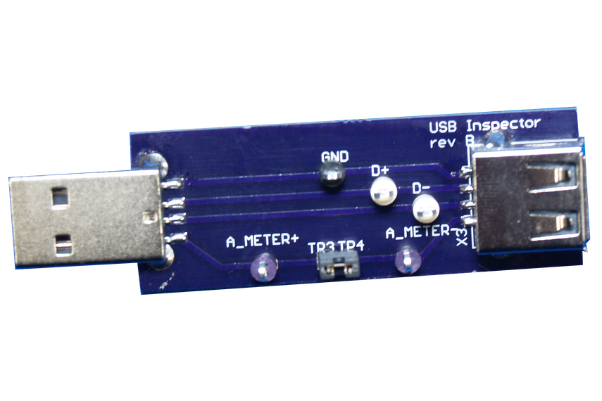

USB Inspector
Image Copyright - Misperry via Tindie

https://www.tindie.com/products/misperry/usb-inspector/?pt=full_prod_search

I also found this product on tindie which is similar but has a current monitoring circuit built in:

https://www.tindie.com/products/Kaktus/usbuddy-usb-development-tool/?pt=full_prod_search

A friend of mine and blog reader found this one:

https://friedcircuits.us/50?search=usb

Either of these products would work for my purposes but the first product's shipping costs from the USA seem a little extravagant and I only wanted one or two.

The second product uses pin headers to allow connection which are a bit close together for my liking. It's often the way of things.  When I cannot obtain what I want I make my own!

The circuit is very simple:


The PCB layout is a little more complicated.  I would like to keep the board as small as possible but maintain the recommended conductor impedance that a USB cable should have.  By maintaining the impedance it means that signals can be correctly measured and power is not needlessly wasted.  The USB specification document is possibly one of the hardest pieces of technical literature I have had to read.  I don't recommend it unless absolutely necessary:

http://www.usb.org/developers/docs/usb20_docs/#usb20spec

There is also a standard for USB cables which dilutes the information into a slightly more readable format (note - I am being overly sarcastic):

BS EN 62680-2-3:2015

The standard is not free to read however...but memberships to local and university libraries yields useful results.

A USB 2.0 cable must have many specifications but the two most critical that I am interested in are:

  • Cable impedance - 76.5 Ω to 103.5 Ω
  • Current carrying capability - 500 mA (standard) or 1.5 A from a dedicated charging port.

The information on the current carrying capability is confusing as there is mention of 5 amps on the wikipedia article:

https://en.wikipedia.org/wiki/USB#Power-use_topology

So based upon the above information we need to ensure the board layout has tracks capable of carrying 1.5 Amps of current at 5 Vdc and that the data pairs D+ and D- are routed as a differential pair with 90 ohms impedance.  I picked 90 ohms as a reasonable middle value and it was cited in this application note from Silicon Labs:

https://www.silabs.com/documents/public/application-notes/AN0046.pdf

Here is a useful article on layout guidelines for differential pairs:

http://www.eetimes.com/document.asp?doc_id=1144365

Basically I want to make sure my breakout board doesn't ruin the USB signals by interrupting them. USB cables are actually proper transmission lines and the cable should be screened and the internal cables twisted to maintain uniform impedance.  The D+ and D- tracks which are differential signals will need to be routed close together above a solid ground plane (Microstrip transmission line) ensuring that both tracks are exactly the same length.  Most PCB routing software like eagle have built in calculators and tools to assist with this.

Here is an excellent (and free) online trace width calculator:

http://www.4pcb.com/trace-width-calculator.html

I entered the following information into the calculator:

  • Current: 1.5 Amps (I'm going with the lower value specified)
  • Copper thickness: 35 µm (Standard 1 oz copper thickness for FR4 PCB material)
  • Temperature Rise: 10 °C (Just a guess)
  • Ambient Temperature: 25 °C (Just a guess)
  • Trace Length: 35 mm (just a guess for now)

I'm only going to have a two layer PCB so I'm only interested in external traces.  Here is what the calculator came up with:

  • Required Trace Width: 525.491 µm or 0.525491 mm
  • Resistance: 33.612 mΩ
  • Voltage Drop: 50.419 mV
  • Power Loss: 75.628 mW

So that sets the PCB track thickness to be at least 0.6 mm.  I may well go with 1 mm as space should not be a problem.

Next we need to set the track impedance above a ground plane which is otherwise known as a microstrip transmission line.  Here is another very useful (and free) calculator:

https://www.eeweb.com/toolbox/edge-coupled-microstrip-impedance

If people need to read up on what an edge coupled microstrip layout is then please check out the link below.  It is essentially a method of setting the impedance of PCB tracks based upon the thickness and width of the track, the thickness of the dielectric material (FR4 PCB) and Wheeler's Equation.

https://en.wikipedia.org/wiki/Microstrip

Transmission line theory is complicated and to be honest I have no intention of attempting to simplify it...I'm not sure that I could.  Basically this is some of the RF black magic people talk about.... I'm trying to keep things simple.  I would suggest that anyone who is serious about electronics and electrical signal propagation needs to have a basic understanding of transmission line theory and how to layout PCB tracks to properly interface connectors with circuits.

Here is what I fed into to the calculator:

Trace Thickness: 35 µm (Standard 1 oz copper thickness for FR4 PCB material)
Substrate Height: 1.6 mm (Standard FR4 PCB)
Trace Width: 1.5 mm (I chose 1 mm value above but went for 1.5 mm to get the right impedance)
Trace Spacing: 0.12 mm (I chose this value as a guess after trying a few different values)
Substrate Dielectric: 4 (This is the relative permittivity of FR4 PCB material)

The calculated result gives a differential impedance of 89.8 Ω - close enough!  So all that's needed is to set the D+ and D- tracks to be 0.12 mm apart and 1.5 mm thick and try to keep the tracks the same length...If we manage that we have the 89.8 Ω impedance needed to ensure that the USB signals remain unaffected when we use the PCB.

Now that we have all of the track properties calculated we can design the PCB layout.  There is a tool in Eagle for doing this that ensures that the differential tracks are routed together.  You have to label the net names with an 'underscore P' and an 'underscore N'.  I set the label for my D+ and D- nets to 'TEST_P' and 'TEST-_N' but any sensible names will do.  I then routed the +V and GND tracks manually and then set the autorouter to route the top layer.  I cannot seem to get the differential pair tool to work otherwise.  Here is what the board layout looks like:


Edit - I have updated the design after some valuable feedback from Aamir Ahmed Khan (Thank you!) - I did not remember to set the track separation distance in my original layout, I have rectified that and my calculations.  Here is the new and now hopefully correct layout.  (Note to self - I should not rush when designing PCB layouts and writing informative blog posts!).  I found the easiest way to do this was to set the grid to 0.2 mm spacing with the alternative at 0.1 mm and route the differential tracks by hand one after the other.  That enabled me to ensure the tracks were correctly separated and of the correct thickness.  I also set the ground plane isolation to be 0.2 mm to ensure the track on the bottom layer was correctly isolated...Lets see if this works!  I hope the PCB fabricators are able to etch the board for me with such precise track isolation...I can always run a scalpel down the gap though.

I will probably get the whole thing manufactured by Elecrow and for that I will need a bill of materials.

Qty Device Package Parts Vendor Part Number Description


1 USB 2.0 Socket USB X1 Farnell 2134385 AMP USB 2.0 connector
4 Ring_Test 1X01_LONGPAD +V, D+, D-, GND Ebay.co.uk 292175228920 Ring Test Connector
1 M02PTH3 1X02_LONGPADS JP7 Farnell 3418285 Standard 2-pin 0.1" header pins
1 USB 2.0 Connector USB-A-H JP1 Farnell 1696544 USB Connectors


Here is the PCB render:


My plan is to have ten boards made, keep two for myself and flog the rest!

That's all for now - Langster!