Showing posts with label USB. Show all posts

Tuesday, 1 August 2017

Designing A USB Breakout Board!

I often need to intercept USB signals for decoding and measurement purposes.  I cut a cable apart last time I needed one but to be honest I much prefer doing things properly.  I also noticed that nobody seems to sell a similar product on Ebay, Aliexpress or Amazon!  I did find a vendor in the USA on tindie:


USB Inspector
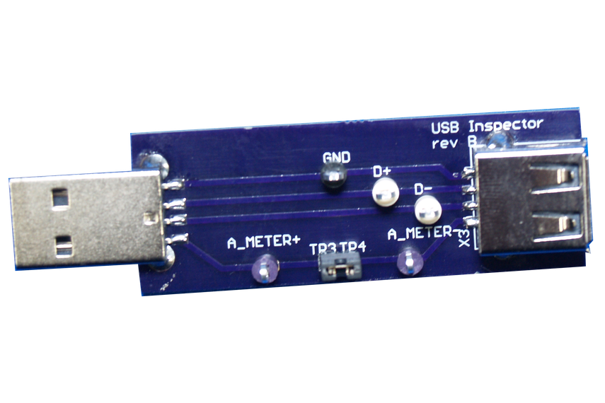
Image Copyright - Misperry via Tindie

https://www.tindie.com/products/misperry/usb-inspector/?pt=full_prod_search

I also found this product on tindie which is similar but has a current monitoring circuit built in:

https://www.tindie.com/products/Kaktus/usbuddy-usb-development-tool/?pt=full_prod_search

A friend of mine and blog reader found this one:

https://friedcircuits.us/50?search=usb

Either of these products would work for my purposes but the first product's shipping costs from the USA seem a little extravagant and I only wanted one or two.

The second product uses pin headers to allow connection which are a bit close together for my liking. It's often the way of things.  When I cannot obtain what I want I make my own!

The circuit is very simple:


The PCB layout is a little more complicated.  I would like to keep the board as small as possible but maintain the recommended conductor impedance that a USB cable should have.  By maintaining the impedance it means that signals can be correctly measured and power is not needlessly wasted.  The USB specification document is possibly one of the hardest pieces of technical literature I have had to read.  I don't recommend it unless absolutely necessary:

http://www.usb.org/developers/docs/usb20_docs/#usb20spec

There is also a standard for USB cables which dilutes the information into a slightly more readable format (note - I am being overly sarcastic):

BS EN 62680-2-3:2015

The standard is not free to read however...but memberships to local and university libraries yields useful results.

A USB 2.0 cable must have many specifications but the two most critical that I am interested in are:

  • Cable impedance - 76.5 Ω to 103.5 Ω
  • Current carrying capability - 500 mA (standard) or 1.5 A from a dedicated charging port.

The information on the current carrying capability is confusing as there is mention of 5 amps on the wikipedia article:

https://en.wikipedia.org/wiki/USB#Power-use_topology

So based upon the above information we need to ensure the board layout has tracks capable of carrying 1.5 Amps of current at 5 Vdc and that the data pairs D+ and D- are routed as a differential pair with 90 ohms impedance.  I picked 90 ohms as a reasonable middle value and it was cited in this application note from Silicon Labs:

https://www.silabs.com/documents/public/application-notes/AN0046.pdf

Here is a useful article on layout guidelines for differential pairs:

http://www.eetimes.com/document.asp?doc_id=1144365

Basically I want to make sure my breakout board doesn't ruin the USB signals by interrupting them. USB cables are actually proper transmission lines and the cable should be screened and the internal cables twisted to maintain uniform impedance.  The D+ and D- tracks which are differential signals will need to be routed close together above a solid ground plane (Microstrip transmission line) ensuring that both tracks are exactly the same length.  Most PCB routing software like eagle have built in calculators and tools to assist with this.

Here is an excellent (and free) online trace width calculator:

http://www.4pcb.com/trace-width-calculator.html

I entered the following information into the calculator:

  • Current: 1.5 Amps (I'm going with the lower value specified)
  • Copper thickness: 35 µm (Standard 1 oz copper thickness for FR4 PCB material)
  • Temperature Rise: 10 °C (Just a guess)
  • Ambient Temperature: 25 °C (Just a guess)
  • Trace Length: 35 mm (just a guess for now)

I'm only going to have a two layer PCB so I'm only interested in external traces.  Here is what the calculator came up with:

  • Required Trace Width: 525.491 µm or 0.525491 mm
  • Resistance: 33.612 mΩ
  • Voltage Drop: 50.419 mV
  • Power Loss: 75.628 mW

So that sets the PCB track thickness to be at least 0.6 mm.  I may well go with 1 mm as space should not be a problem.

Next we need to set the track impedance above a ground plane which is otherwise known as a microstrip transmission line.  Here is another very useful (and free) calculator:

https://www.eeweb.com/toolbox/edge-coupled-microstrip-impedance

If people need to read up on what an edge coupled microstrip layout is then please check out the link below.  It is essentially a method of setting the impedance of PCB tracks based upon the thickness and width of the track, the thickness of the dielectric material (FR4 PCB) and Wheeler's Equation.

https://en.wikipedia.org/wiki/Microstrip

Transmission line theory is complicated and to be honest I have no intention of attempting to simplify it...I'm not sure that I could.  Basically this is some of the RF black magic people talk about.... I'm trying to keep things simple.  I would suggest that anyone who is serious about electronics and electrical signal propagation needs to have a basic understanding of transmission line theory and how to layout PCB tracks to properly interface connectors with circuits.

Here is what I fed into to the calculator:

Trace Thickness: 35 µm (Standard 1 oz copper thickness for FR4 PCB material)
Substrate Height: 1.6 mm (Standard FR4 PCB)
Trace Width: 1.5 mm (I chose 1 mm value above but went for 1.5 mm to get the right impedance)
Trace Spacing: 0.12 mm (I chose this value as a guess after trying a few different values)
Substrate Dielectric: 4 (This is the relative permittivity of FR4 PCB material)

The calculated result gives a differential impedance of 89.8 Ω - close enough!  So all that's needed is to set the D+ and D- tracks to be 0.12 mm apart and 1.5 mm thick and try to keep the tracks the same length...If we manage that we have the 89.8 Ω impedance needed to ensure that the USB signals remain unaffected when we use the PCB.

Now that we have all of the track properties calculated we can design the PCB layout.  There is a tool in Eagle for doing this that ensures that the differential tracks are routed together.  You have to label the net names with an 'underscore P' and an 'underscore N'.  I set the label for my D+ and D- nets to 'TEST_P' and 'TEST-_N' but any sensible names will do.  I then routed the +V and GND tracks manually and then set the autorouter to route the top layer.  I cannot seem to get the differential pair tool to work otherwise.  Here is what the board layout looks like:


Edit - I have updated the design after some valuable feedback from Aamir Ahmed Khan (Thank you!) - I did not remember to set the track separation distance in my original layout, I have rectified that and my calculations.  Here is the new and now hopefully correct layout.  (Note to self - I should not rush when designing PCB layouts and writing informative blog posts!).  I found the easiest way to do this was to set the grid to 0.2 mm spacing with the alternative at 0.1 mm and route the differential tracks by hand one after the other.  That enabled me to ensure the tracks were correctly separated and of the correct thickness.  I also set the ground plane isolation to be 0.2 mm to ensure the track on the bottom layer was correctly isolated...Lets see if this works!  I hope the PCB fabricators are able to etch the board for me with such precise track isolation...I can always run a scalpel down the gap though.

I will probably get the whole thing manufactured by Elecrow and for that I will need a bill of materials.

Qty Device Package Parts Vendor Part Number Description


1 USB 2.0 Socket USB X1 Farnell 2134385 AMP USB 2.0 connector
4 Ring_Test 1X01_LONGPAD +V, D+, D-, GND Ebay.co.uk 292175228920 Ring Test Connector
1 M02PTH3 1X02_LONGPADS JP7 Farnell 3418285 Standard 2-pin 0.1" header pins
1 USB 2.0 Connector USB-A-H JP1 Farnell 1696544 USB Connectors


Here is the PCB render:


My plan is to have ten boards made, keep two for myself and flog the rest!

That's all for now - Langster!

Tuesday, 14 January 2014

mbed SD Card tutorial

I have been playing with the mbed microcontroller again.  I'm really liking this particular microcontroller development platform!  The potential is huge for what can be achieved with this thing.  The only thing I continually struggle with is the documentation.  Whilst the mbed website is good there are still issues that cause the inexperienced to become frustrated...myself included!

One of the most common tasks I need a microcontroller to perform is to log data from instrumentation.  The best way I know of currently doing that is to use an SD card.  I have done this with an arduino so often I almost can do it without thought.  At the moment I am developing some instrumentation with the mbed and need to achieve the same thing - I need a way of logging data measurements.  The data will be stored as text files in ASCII.  I will probably use comma separated values....It makes it easy to import into a spreadsheet or graphing program of choice.

If you are going to try this you will need the following:

An mbed and mini USB cable
An SD card - partitioned and formatted for use on your operating system of choice
An SD card breakout board - try Adafruit or Sparkfun for all your breakout needs!
Some connection wire
Patience!


So I looked at the mbed documentation on the website and searched for SD card tutorial.  A lot of pages appeared but nothing that actually shouted this is how to connect an SD card, here is the circuit diagram and how to connect it up and here is the demonstration code with an explanation of how things work....

https://mbed.org/search/?type=&q=SD+card+tutorial - a lot of pages but nothing definitive

What I actually needed to find was here:


The mbed cookbook is useful but often difficult to navigate - a work in progress.

There is a lot of information on the programming of the mbed - libraries and usage but no pictures on how to connect things up and no schematics.  Lets remedy that!


SD cards normally communicate with the host microcontroller via the SPI protocol - Serial Peripheral Interface.  The mbed has two SPI ports - pins 5, 6 and 7 - MOSI, MISO and SCK and pins 11,12 and 13 - also MOSI, MISO and SCK.  You can use either three pins but they are not interchangeable.  In my testing I used 11,12 and 13 because I have already made plans for pins 5 and 7!

Here is a picture of the connections:


I used an SD breakout board so my connections are a little different from the above schematic.  I am connecting +5V to Vdd because my breakout board has a logic level converter to convert 5V to 3.3V.  The breakout board was designed for use with TTL logic based microcontrollers like the arduino.  If you are using just an SD card connector the information in the schematic is correct.  Change your connections to suit your breakout board as necessary.

Once I had checked and rechecked my connections!  I keep having to do that at the moment - I imported the example code into the online compiler and then uploaded it to my mbed

Here is the the link to the example code again so people can find it easily:


It should compile with no errors.  Ensure that you update the code with the relevant information with where you have made the connections.  If like me you are using pins 11, 12 and 13 for MOSI, MISO and SCK you need to change the line highlighted to reflect that.

#include "mbed.h"
#include "SDFileSystem.h"

SDFileSystem sd(p11, p12, p13, p8, "sd"); // the pinout on the mbed Cool Components workshop board

int main() {
    printf("SD card test!\r\n");   

    mkdir("/sd/mydir", 0777);
    
    FILE *fp = fopen("/sd/mydir/sdtest.txt", "w");
    if(fp == NULL) {
        error("Could not open file for write\r\n");
    }
    fprintf(fp, "Hello fun SD Card World!\r\n");
    fclose(fp); 

    printf("File successfully written and closed!\r\n");
}

I suppose I should try and explain what the code does:

The first line tells the compiler to include the core header file for the mbed and the second include statement tells the compiler to use the header file containing the instructions relating to SD cards.

The third line SDFileSystem sd(p11, p12, p13, p8, "sd");  tells the compiler that the SD card is connected to pins 11, 12 , 13 and pin 8. 

NB - Pin 8 is the control line for the SD card it's known as CS or SS depending on which information you read or what is printed on the breakout boards silk screen - mine was SS.

The rest of the code prints a message to the mbed com port, makes a directory on the SD card and then creates a text file called sdtest.txt.  If for some reason the file cannot be created or opened an error message is displayed on the serial terminal; the program then finishes.  If the file was created and opened successfully a message will be written inside the text file and then the test file is closed. A further message is sent to the serial terminal to document the program's success.

I use a free terminal program called PuTTy for my serial, Telnet or SSH requirements.  It is a great piece of software!  You can get it from here:


I suggest people try it out - it's useful...

Anyway...back to the cool stuff.  Connect up your mbed to your PC and copy the compiled .bin file to your mbed and press the reset button.  If all is well the blue power / programming LED will flash and then the program will exit.  No other LEDs should be illuminated.  

If you load up PuTTy and point it towards your mbed serial terminal with the settings:

COMXX - 9600, n, 8, 1 with no flow control - where XX is the COM port number of your mbed you can view the output:


Open the terminal window and view the results...


Actually that was amazing for me...I couldn't get this to work for love nor money at first - I'm losing my touch!

If you remove your SD card and view it in a file explorer there will be a new directory on your SD card called mdir and inside this folder there will be a text file called sdtest.txt.  Open it and verify it is all correct.

If things are wrong and they often are...then the four LEDS at the bottom of the mbed will flash from outer to inner and the following messages will be shown in PuTTy:


The flashing LEDS of SD card failure...


If you see this then unfortunately something is wrong either with the wiring, the SD card or your mbed.  In my case I was struggling for a long time because I was using the unregulated +5V input to power the SD card.  My computer couldn't power both the mbed and the SD card.  As soon as I swapped to the regulated +5V everything worked perfectly.  If it doesn't work for you, all I can suggest is check check and re-check connections and then ask for help!  I didn't but perhaps I should have...I even checked the MOSI, MISO and SCK where occurring using an oscilloscope and a logic analyser.  I re-wired at least ten times and checked continuity with a multimeter.  It wasn't until I measured the voltages with a digital multimeter that I noticed that there was not enough voltage to power the SD card.  If I had been using a breakout board without a logic level converter and wired as shown in the schematic diagram this would have worked first time....No matter - all is working and well now and more information and confidence gained - bonus!

There are so many reasons to want to log data to external memory with microcontrollers - it's the corner stone of instrumentation.  I'm going to turn this into a memory stick of sorts so that I just have to connect a USB cable to the mbed (not the programming cable) so that I can browse the SD card data!  Simples!

That's all for now people - take care

Langster!