The display itself could be any 16x2 LCD display but I bought one especially from Numato labs as it makes it more simple to connect to the Mimas V2 FPGA development board.
Here is a picture of the display:
 |
| 16x2 LCD displays with onboard 5V regulator |
LCD Expansion Module User Manual
The manual provides information on the LCD display has been constructed and how it should be used and connected to an FGPA development board such as the Elbert V2 or Mimas V2 FPGA development boards. The pin connections are below:
 |
| 16x2 Expansion LCD Pin Connections |
The display has been physically designed to connect to one of the spare input header sockets on the Elbert or Mimas V2 FPGA development boards. It could be connected to any FPGA development board or Micro-controller however as long as the pin connections are known.
 |
| LCD Display Connected to the P6 Header socket on the Mimas V2 |
LCD Display16x2 Example project
Download the example project and uncompress it to a folder of your choice.
The project has been written in verilog which I'm not too familiar with. I am slowly learning VHDL for when I use FPGAS however verilog is similar and I know the code works as intended. If we load the project up in Xilinx WebISE we are presented with the following:
The first thing required is to change the project settings to relate to the FPGA device on the Mimas V2 development board. At the moment it is set for use with an Elbert V2 development board. Right click on the project hierachy box and select "Design Properties":
Then change all of the information in the windows that opens to match the picture below:
 |
| Mimas V2 Design Properties for LCD Example project |
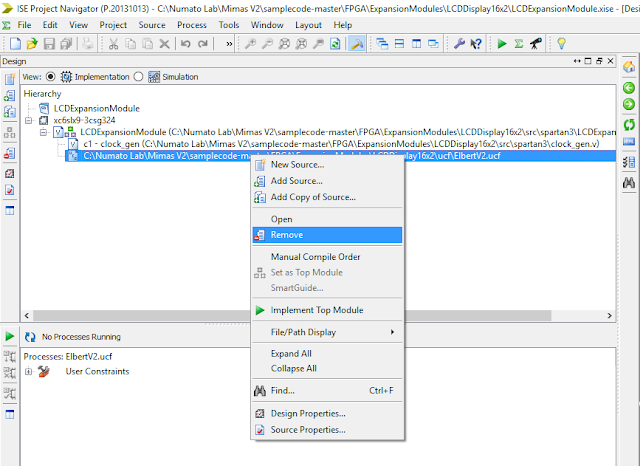
Right click on the UCF file and remove it from the project:
Click on 'Yes' when the confirmation window is displayed.
Now right click on the project hierachy box and select "Add Source"and then navigate to the UCF folder where the project was unzipped on your hard disk. Select the UCF file called MimasV2.ucf and click 'Open' and then click 'Ok' on the confirmation windows that appear.
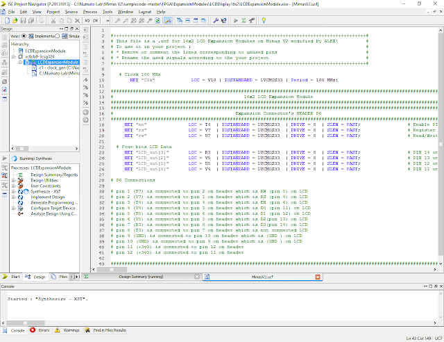
Now double click on the newly added UCF file to open in for editing in Xilinx WebISE:
Here is where things get interesting. I looked at the pin labels on P6 of the Mimas V2 Development board and the pin labels on the LCD expansion PCB. I found that Row 1 of the Development board is connected to Row 2 of the LCD expansion PCB and that Row 2 of the Development board was connected to Row 1 of the LCD Expansion PCB. Because these are reversed the supplied UCF file is unfortunately not correct. I verified this with a multimeter (and a lot of patience) and re-wrote the UCF file to create the correct connections:
#+++++++++++++++++++++++++++++++++++++++++++++++++++++++++++++++++++++++++++++++++++++++++++#
# This file is a .ucf for 16x2 LCD Expansion Modules on Mimas V2 modified by ALEX! #
# To use it in your project : #
# * Remove or comment the lines corresponding to unused pins #
# * Rename the used signals according to the your project #
#+++++++++++++++++++++++++++++++++++++++++++++++++++++++++++++++++++++++++++++++++++++++++++#
# Clock 100 MHz
NET "Clk" LOC = V10 | IOSTANDARD = LVCMOS33 | Period = 100 MHz;
####################################################################################################################################################
# 16x2 LCD Expansion Module #
####################################################################################################################################################
####################################################################################################################################################
# Expansion Connector's HEADER P6 #
####################################################################################################################################################
NET "en" LOC = T4 | IOSTANDARD = LVCMOS33 | DRIVE = 8 | SLEW = FAST; # Enable PIN of LCD
NET "rs" LOC = V7 | IOSTANDARD = LVCMOS33 | DRIVE = 8 | SLEW = FAST; # Register Select PIN of LCD
NET "rw" LOC = U7 | IOSTANDARD = LVCMOS33 | DRIVE = 8 | SLEW = FAST; # Read/Write PIN of LCD
# Four bits LCD Data
NET "LCD_out[3]" LOC = R3 | IOSTANDARD = LVCMOS33 | DRIVE = 8 | SLEW = FAST; # PIN 14 on LCD
NET "LCD_out[2]" LOC = V5 | IOSTANDARD = LVCMOS33 | DRIVE = 8 | SLEW = FAST; # PIN 13 on LCD
NET "LCD_out[1]" LOC = U5 | IOSTANDARD = LVCMOS33 | DRIVE = 8 | SLEW = FAST; # PIN 12 on LCD
NET "LCD_out[0]" LOC = V4 | IOSTANDARD = LVCMOS33 | DRIVE = 8 | SLEW = FAST; # PIN 11 on LCD
# P6 Connections
# pin 1 (U7) is connected to pin 2 on header which is RW (pin 5) on LCD
# pin 2 (V7) is connected to pin 1 on header which is RS (pin 4) on LCD
# pin 3 (T4) is connected to pin 4 on header which is EN (pin 6) on LCD
# pin 4 (V4) is connected to pin 3 on header which is D0 (pin 11) on LCD
# pin 5 (U5) is connected to pin 6 on header which is D1 (pin 12) on LCD
# pin 6 (V5) is connected to pin 5 on header which is D2(pin 13) on LCD
# pin 7 (R3) is connected to pin 8 on header which is D3(pin 14) on LCD
# pin 8 (T3) is connected to pin 7 on header which is not connected LCD
# pin 9 (GND) is connected to pin 10 on header which is (GND ) on LCD
# pin 10 (GND) is connected to pin 9 on header which is (GND ) on LCD
# pin 11 (+3v3) is connected to pin 12 on header
# pin 12 (+3v3) is connected to pin 11 on header
####################################################################################################################################################
Copy and paste the above code into the UCF text editor and save the project.
Now it's time to compile the project and generate a bit file ready to upload to the Mimas V2 Development board. Click on the green Arrow in the middle of the screen to compile the project:
Once that is complete generate a 'Bit File' and then upload that to the Mimas V2 Development board via your preferred method - by Python Script or by using the supplied uploader. I use the uploader.
Ensure you have a power supply connected to the Vext input of the Expansion PCB (which is capable of supplying at least 7 Volts. When you connect it up you should be presented with the following images:
I know they are upside down but it does prove the display is working!
If you wish to change the message that is displayed on the LCD then the following lines of code will be of interest:
// Shift the display right.
assign memory[19]={2'b00,8'h1C};
// Character that should be displayed on the LCD.
assign memory[20]={2'b10,"W"};
assign memory[21]={2'b10,"E"};
assign memory[22]={2'b10,"L"};
assign memory[23]={2'b10,"C"};
assign memory[24]={2'b10,"O"};
assign memory[25]={2'b10,"M"};
assign memory[26]={2'b10,"E"};
assign memory[27]={2'b10," "};
assign memory[28]={2'b10,"T"};
assign memory[29]={2'b10,"O"};
// Shift to second Line of LCD
assign memory[30]={2'b00,8'h40};
// Space that should appear on LCD.
assign memory[31]={2'b10," "};
// Shift the display right
assign memory[32]={2'b00,8'h1C};
// Character that should be displayed on the LCD.
assign memory[33]={2'b10,"N"};
assign memory[34]={2'b10,"U"};
assign memory[35]={2'b10,"M"};
assign memory[36]={2'b10,"A"};
assign memory[37]={2'b10,"T"};
assign memory[38]={2'b10,"O"};
assign memory[39]={2'b10," "};
assign memory[40]={2'b10,"L"};
assign memory[41]={2'b10,"A"};
assign memory[42]={2'b10,"B"};
The first line shifts the display right by three characters. As the display has availability for 16 characters in each line this places the first character to be displayed at position 4 on the first line.
The next ten lines assign the memory register with characters to be displayed. If you wanted to these can be changed to whichever ascii character required. Change the characters in the quotation marks but remember that a space must be " " and not "". Using "" causes three horizontal lines to be displayed. I changed the code to that displayed below:
// Shift the display right.
assign memory[19]={2'b00,8'h1C};
// Character that should be displayed on the LCD.
assign memory[20]={2'b10,"V"};
assign memory[21]={2'b10,"E"};
assign memory[22]={2'b10,"R"};
assign memory[23]={2'b10,"I"};
assign memory[24]={2'b10,"L"};
assign memory[25]={2'b10,"O"};
assign memory[26]={2'b10,"G"};
assign memory[27]={2'b10," "};
assign memory[28]={2'b10,"I"};
assign memory[29]={2'b10,"S"};
// Shift to second Line of LCD
assign memory[30]={2'b00,8'h40};
// Space that should appear on LCD.
assign memory[31]={2'b10," "};
// Shift the display right
assign memory[32]={2'b00,8'h1C};
// Character that should be displayed on the LCD.
assign memory[33]={2'b10,"H"};
assign memory[34]={2'b10,"A"};
assign memory[35]={2'b10,"R"};
assign memory[36]={2'b10,"D"};
assign memory[37]={2'b10," "};
assign memory[38]={2'b10,"T"};
assign memory[39]={2'b10,"O"};
assign memory[40]={2'b10,"U"};
assign memory[41]={2'b10,"S"};
assign memory[42]={2'b10,"E"};
I then re-compiled the code and re-uploaded it to the Mimas V2 Development board. Here is what I got:
In order to reduce the number of spaces at the beginning the lines:
assign memory[19]={2'b00,8'h1C};
assign memory[32]={2'b00,8'h1C};
must be changed to suit the requirements. The section 2'b00 section sets the RS and RW registers to zero. Setting the RS register to zero means the display is being sent a command by the FPGA. The RW pin is 0 when sending information to the display and 1 when displaying items on the display. I am not sure what the h1C part of the code performs.
I have found that by changing the line to
assign memory[19]={2'b00,8'h1B};
moves the text starting position to the first block on the display. I also increased the amount of memory present in the register by changing this line from 43 to 44:
// Specify the depth of block memory where the data and command are to be saved.
parameter Length=44;
That allowed me to obtain the following result:
That's all for now. I will investigate further as to how this code works.
Take care - Langster


I examine your blog site presently share great information right below.
ReplyDelete