Saturday, 25 October 2014

Simple Flyback Driver

I was searching in my junk pile - every engineer should have one of those!! I found a flyback transformer from an old CRT television.


These are used to generate the very high voltage required to energise the tube in a cathode ray television or monitor.  Anyway I decided to make a 'Jacob's ladder' high voltage circuit with it.  This is a fancy display circuit which shows a rising high voltage arc between two conductors.

A Jacob's Ladder in Operation
WARNING!  This project is potentially dangerous and should not be attempted by people without high voltage experience!  Anything that happens to you is not the Author's fault in anyway in the event of misuse of the information contained within this post!  This includes being responsible for any bodily damage or property damage that is a result of building or using this circuit. High voltage can be dangerous or lethal when used incorrectly.  It is up to the user of the circuit to ensure their safety when using high voltage equipment at all times.

There are plenty of pages related to this project and I used quite a few of them researching this post:

Instructables flyback driver

Loneocean's Flyback Drivers page

Plasmana's Instructable on an FET based Flyback

Most of the circuits found use a simple but power 2N3055 transistor circuit in a self oscillation mode which energises a flyback transformer to create the spark.  Here is the circuit:


This circuit does work once you get the connections to the primaries of the Flyback Transformer correctly wired.  I found that the power supply required had to be incredibly high current and the transistor failed after only ten uses.  It also generated so much heat some of the components melted the solder connecting them to the wires!!!  I had a heatsink on the transistor that took fifteen minutes too cool down.  Because of this I decided to simulate the circuit and see how much power is generated in each section...


I really like circuit simulators...they help show whats going on without having to build a circuit and destroy things...They also let you attach oscilloscopes to really high voltage outputs without destroying the oscilloscope.  I couldn't do this in real life without a high voltage probe....which I don't currently have!

Blue trace = HV output, Red trace = Transistor Collector, Green trace = Transistor Base 


Expanded Oscillocope output
The circuit simulator helpfully automatically calculates the voltage and current present in each part of the circuit.  The peak voltage generated at the output into practically no load (an oscillocope) shows almost 100kV (100,000V)!!!  That is huge and quite awesome....the sparks would be amazing!  There is just one problem.  The voltage and current applied to the Transistor collector is also very high...204V and 20.3A - that's 4141.2 Watts or 4kW....most electric heaters only draw 1kW....this thing draws enough power to heat a large room!  The base terminal also receives far too much power 236V and 3.68A which gives 868.48 Watts.  I haven't checked but I suspect that the transistor is not designed to contain that kind of energy and function correctly for long....which is probably why when I tried this circuit it didn't work for long....*Sad Face*

Rather than dwell on my failures...I decided to redesign the circuit to prevent the transistor failing and reduce the amount of circuit current present whilst compromising on the amount of high voltage present at the output * Slightly less sad face *

Here is my newly designed circuit which uses slightly newer and more easily available components:


I also designed a PCB to mount the components to and because I find designing PCBS easier than using veroboard...Here is the bottom layer with the tracks:


Here is the component placement:


If you would like to make this project yourself you will need the following components:

1x 1k Ohm Resistor 1/4 Watt
1x 2k2 Ohm Resistor 1/4 Watt
1x 330 Ohm Resistor 1 Watt

2x UF4007 Diode
1x 1N5375 Zener Diode
1x IRF631 N-Channel Field Effect Transistor or Similar - IRF540 works well!

1x SK104 Heatsink or similar

3x 5mm Screw terminal connectors (you can just solder the wires)

1x PCB or veroboard - Ebay or Farnell (use my design or make your own!)

1x Flyback transformer - Ebay

Some thick (24 gauge) enamel coated wire - at least a metre off

The circuit is a version of a classic flyback driver circuit used for driving neon lights and compact fluorescent lighting tubes.  I have designed it to provide some reasonable sparks whilst preventing the switching transistor from getting too hot.

The circuit works by applying voltage to the primary winding and at the same time applying a lower voltage to the secondary winding.  The voltage on the seconddary winding applied to the gate of the FET allows voltage to flow from the drain of the FET to the source and to 0V.  Once this occurs the FET turns off and the process repeats.  This action causes a pseudo square wave to be driven through the Flyback transformer which energises it and generates a very high voltage but low current spike at the output winding.  This a self resonant circuit - the switching frequency is dependent of the transistor and the number of windings on the primary and secondary of the Flyback transformer.  The Zener diode and UF4007 diodes protect the field effect transistor from too much voltage being applied to the gate and drain terminals.  The capacitor is there to help stabilize the circuit oscillation.

The simulation of the circuit shows that the current present at the gate and drain of the N-Channel FET is now much more acceptable:


Before we can use this circuit we need to wind our primary and secondary of the input to the flyback transformer:


I covered the exposed primary core with insulating tape and then wound ten turns or wire for the primary and 5 turns of wire for the secondary.  I then cleaned the enamel off the exposed ends and tinned them with solder.

I then had to locate which pins on the flyback transformer were connected to the HV winding so that I know where the spark at the suction cup will arc to.  I used the method outlined here:

How to find the output of a flyback TX

I then connected the flyback transformer to the screw terminal outputs of the driver circuit:


As you can see from the photo I soldered a white wire to the pin of my flyback transformer output and crimped a pin on the other end.  This pin will become damaged with use.  I also taped the HV cup to the bench to prevent it moving.  I don't want to be electrocuted by moving HV!  Safety first!!! Prepare the area where you are going to use the circuit - remove anything flamable and wear goggles and be sensible!

I then connected it to a high current 24Vdc Power supply and turned it on.  At first nothing happened...I then swapped the input windings on the flyback driver and a whistling sound could be heard....I then carefully moved the white wire close to the suction cup and....

SUCCESSFUL HV ARC!!!
Here is a short video of it working...please excuse the cackling...I was having fun!


I have not as yet turned it into a Jacob's ladder which involves connecting the HV suction cup and the white wire to some exposed single core wire bent to a U shape and placed close to each other.  When I do and it's working satisfactorily I will post a video and images.

Please be very careful if you are going to try and reproduce this circuit and be very careful with High voltage electricity - Langster!


Thursday, 16 October 2014

mbed CAN Bus Tutorial

I have been helping some colleagues with their projects particularly with communications protocols. There are many communications protocols currently in use and one of the most popular is known as CAN Bus (Controller Area Network).  Its a serial based communications protocol developed by Bosch.  It is primarily used in the automotive industry.  Modern cars and their associated accessories contain a lot of sensors and feedback systems.  These sensors and systems all need to talk to each other reliably and quickly and because of this CAN bus was developed.  You can read more about CAN bus on Wikipedia here:

CAN Bus Wikipedia Enry

Here are a few other pages which might be of interest:

http://canbuskit.com/what.php

http://www.canbus.us/

http://www.kvaser.com/can-protocol-tutorial/

The topic is quite dry to say the least.  I'm not going to go into the detail about CAN Bus but rather very briefly explain what it does and how it works and then provide an example.  In a modern vehicle the instrument panel communicates with a central microcontroller inside the engine known as the Engine Control Unit or ECU. The ECU is also communicating with sensors inside the engine so that the vehicle speed, gear, engine temperature, oil temperature, coolant temperature etc are all known.  This information from the sensors is used to control the engine and is displayed via the instrument panel. The way this data is communicated uses CAN Bus.

CAN Bus is a two wire protocol - messages are sent as frames on two conductors known as CAN H and CAN L (CAN High and CAN Low).  Although more often a four wire system is used where power and ground are also present.

The speed of communications governs the length of cable between the master and nodes.  For the top speed of 1Mbit/Sec this is 40 metres in length or less.  If less speed is required the length of the cable can be longer.

Can Bus Maximum Length
Bus SpeedBus Length
(L)
Cable Stub Length (l)Node Distance
(d)
1 Mbit/Sec40 meters
(131 feet)
0.3 meters
 (1 foot)
40 meters
(131.2 feet)
500 kbits/Sec100 meters
(328 feet)
 0.3 meters
 (1 foot)
100 meters
(328 feet)
100 kbits/Sec500 meters
(1640 feet)
0.3 meters
 (1 foot) 
500 meters
(1640 feet)
50 kbits/Sec1000 meters
(3280 feet)
 0.3 meters
 (1 foot)
1000 meters
(3280 feet)

Information from the 1st node to the 2nd node is sent in frames (packets of information).  There are four different types of frame - Data, Remote, Error and Overload.

A Frame itself is made up of bits (ones and zeros in a pattern).

If you were to look at a frame using a logic analyser you might see something like this:

The start of the frame the logic goes from High to Low to High (transition).  The identifier is sent next (a specific code made up of highs and lows which tell the receiver what type of frame it is...this is followed by another high to low to high transition known as the RTR - ready to receive.  That whole section is known as the arbitration field - it tells the receiver what kind of frame has been received and that the receiver needs to respond.  The next section is called the control field which is followed by the data field.  After that a cyclic redundancy check (CRC) is performed to ensure that the data was received correctly.  Lastly an acknowledge transition to mark the end of the frame is seen.

Rather than concentrate on the theory of operation lets discuss how to implement a CAN Bus system using the mbed microcontroller - you will need two mbeds, a length of 2 core wire, 2x 120R resistors and hookup wires.  You will also need two CAN Bus tranceivers - there are many different versions of these devices available.  I'm using the MCP2551 from Microchip.  A CAN Bus tranceiver is an eight pin integrated circuit designed to transmit and receive CAN Bus messages.  The link to the datasheet for the MCP2551 is below:

MCP2551 datasheet

Lets implement a simple circuit which flashes an LED when a valid message sent from one node and when this message is received by another node a different LED flashes.


Here is how are how things looks when the above circuit is implemented:

1st mbed - The CANbus Transmitter
2nd mbed - The CANbus Receiver

I'm going to use a length of multicore alarm cable to connect both microcontrollers together making up the 'CAN Bus'.  However if you wanted you could just use two short wires and have both mbeds on the same breadboard:

Both mbeds - ready to go!
Here is the Transmitter code - this needs to be uploaded to the first mbed:

/* 
Transmitter code
CANBus Tutorial based on lots of example code
*/

#include "mbed.h"
Serial pc(USBTX, USBRX);          // tx, rx for Tera Term output

DigitalOut led1(LED1);            // LED1 displays messsage sent Status
CAN can1(p9, p10);                // CAN interface
char counter = 0;                 // Counter Variable to store number of sent messages

int main() {
  printf("sending a message via CANbus... ");
  while (1) {       
    // send value to CAN bus and monitor return value to check if CAN
    // message was sent successfully. If so display, increment and toggle
    if (can1.write(CANMessage(1, &counter, 1))) {  
       pc.printf("CANBus Message sent: %d\n", counter);       // display message
       counter++;                                             // increment message counter value
       led1 = !led1;                                          // toggle LED1 to show message sent
    }else{
      can1.reset();                                           // Reset CANbus if there is a problem
    }
    wait(1);                                                  // wait a second  
  }
}

Here is the Receiver code - this needs to uploaded to the second mbed:

/* 
Receiver code
CANBus Tutorial based on lots of example code
*/

#include "mbed.h"

Serial pc(USBTX, USBRX);          // tx, rx for Tera Term output
DigitalOut led2(LED2);            // status LED
CAN can1(p30, p29);               // CAN interface

int main() {
  CANMessage msg;                 // create empty CAN message
  printf("received a CANbus message...\n"); // Write to serial terminal
  while(1) {
    if(can1.read(msg)) {          // if message is available, read into msg
      printf("Message received: %d\n", msg.data[0]);   // display message data
      led2 = !led2;                                    // toggle receive status LED
    } 
  }
}

Once the circuits have been constructed and are correctly wired up when you apply power to each mbed you should see LED1 flash on the transmitting mbed and see LED2 flash on the receiving mbed every second.  You can also look at each mbed in a serial terminal and will be able to see the message count being sent and received independently on each mbed!  Cool huh...We can use this comms protocol to do some very useful things!

Here is a picture of the terminal windows showing the serial messages:


Here is a video showing the circuit working....apologies for the wiring issues!


I had real trouble getting this to work...check your wiring very carefully.  The mbed whilst good in principle is very hard to wire up correctly.  I am seriously considering obtaining a decent mbed motherboard to make these tutorials easier for me.  I tried using the Arch-pro mbed from Seeed studios to act as the second mbed but just could not get it to play.  I ended up borrowing another mbed from a friend in order to get things working...anyway that's it.  Take care - Langster!


Sunday, 12 October 2014

Elbert V2 Nand Gate Tutorial

Hi, Here is another tutorial concerning the Elbert V2 FPGA development board.  I'm still working out how to use the board along with the using the Xilinx Webpack IDE.

The previous tutorial is here:

Elbert V2 Not Gate Tutorial

Here is how to implement a 6 input Nand gate using the schematic input section of the IDE.  Not sure why anyone would need a 6 input Nand gate but anyway...

Load up the project navigator by double clicking on ISE Design 14.7 icon:


Start a new project by clicking on the file menu and selecting new project.

The following window will be displayed:


Choose a suitable folder to store your project and select 'schematic' as the source type.  We are going to use the schematic entry system to design our Nand gate.  Click 'Next' to continue:


Enter the details specific to the Elbert V2 FPGA development board, make sure all of the details shown above are correct.  We will be using verilog to implement the design.  Click 'Next' to continue:


The project summary is displayed next - click finish to return to the main part of the IDE:


Right click on the 'Hierarchy' Section and add a new source file, select Schematic and give it a suitable file name:


Click 'Next' and a summary window will be displayed:


Click 'Finish' when ready to continue.  After a few moments the Schematic Editor Screen will be displayed:


Zoom in a little by clicking on the 'magnifying glass icon' on the top toolbar:


Next click on the add parts icon and then select logic for the category and Nand8 for the symbol. Then place the symbol on the design screen:


Add wires to the inputs and the output of the Nand Gate:


Add the wires by left clicking on the gate wire and then drawing a short line before double clicking to end the wire:


Next Add I/O markers to the inputs and outputs using the add I/O marker icon:


The diagram should now look like this:


Double Click on the input arrow 'XLXN_1' - the following window will be displayed, change the name to 'A':


Repeat the process for all of the inputs and outputs - use sensible NET names, I used 'Z' for the output and 'A' to 'H' for the inputs.  The diagram now looks like this:


Click on the 'Design' tab in the bottom left corner of the screen and then select simulation:


Right click on the 'Hierarchy' box and add new source file, select 'verilog test fixture' and give it a suitable file name:


Click 'Next' to continue, after a few moments the following screen will be displayed:


The IDE has helpfully created a test bench file based upon the information in the schematic.  All we need to do is add some extra lines of code to test our implementation of an eight port Nand Gate:

// Initialize Inputs
   initial begin
A = 0;
B = 0;
C = 0;
D = 0;
E = 0;
F = 0;
G = 0;
H = 0;
#10 // Wait ten nano seconds
A = 1; // Set the A input high
#10 // Wait ten nano seconds
B = 1; // Set the B input high
#10 // Wait ten nano seconds
C = 1; // Set the C input high
#10 // Wait ten nano seconds
D = 1; // Set the D input high
#10 // Wait ten nano seconds
E = 1; // Set the E input high
#10 // Wait ten nano seconds
F = 1; // Set the F input high
#10 // Wait ten nano seconds
G = 1; // Set the G input high
#10 // Wait ten nano seconds
H = 1; // Set the H input high
#10 // Wait ten nano seconds
#100 // Wait one hundred nano seconds
$finish; //finish the simulation
end

Remove the 'ifDef auto_init line and the 'endif lines and either copy and paste the above code or type it in....choice is yours.  The screen should look similar to below:


Now is the time to save this file and then run a 'Behaviour check syntax' by right clicking on the 'Design Utilites' and choosing the appropriate option:


Once complete a green tick should be displayed as above.  Now it's time to simulate the behavioural model - select that by right licking on 'Simulate Behavioural Model'  After a few moments the following screen should be displayed:


Click on the 'Default.wcfg' tab to display the waveform from the simulation.  It should look something similar to below:


To expand the waveform and show the edge transitions click on the 'Zoom to full view' icon:


Now that we have proved our design will work it's time to tell the software which pins of the FPGA we would like to connect to the inputs and how we will display the output.  First of all we need to remove the test bench file from the project as it isn't required for the implementation.  Right click on the test bench file and remove it:


Then click on implementation and add a new source file - an 'Implementation Constraints file':


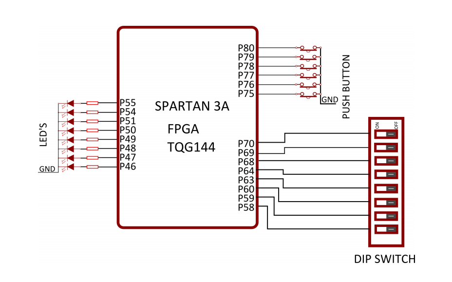
A new file will be opened inside the Xilinx IDE and it will be blank.  We need to add the information required to tell the compiler which FPGA pins we would like to use as inputs and outputs.  If we look at the Elbert V2 Schematic we can see that the development board has some DIP switches available to use as inputs and some LEDS available - lets use an LED for the output and the DIP switches as inputs:


We can see that LED 8 is connected to pin 46 and the DIP switches are connected from Pin 58 to pin Pin 70.  Lets write the 'user constraints file':

CONFIG VCCAUX = "3.3" ;

TIMESPEC TS_CLK = PERIOD "CLK" 12 MHz HIGH 50%;

############################################################################
# LED
############################################################################

    NET "Z"            LOC = P46  | IOSTANDARD = LVTTL | DRIVE = 8 | SLEW = FAST ;

############################################################################
# DP Switches
############################################################################

    NET "A"       LOC = P70  | IOSTANDARD = LVTTL | DRIVE = 8 | SLEW = FAST | PULLUP ;
    NET "B"       LOC = P69  | IOSTANDARD = LVTTL | DRIVE = 8 | SLEW = FAST | PULLUP ;
    NET "C"       LOC = P68  | IOSTANDARD = LVTTL | DRIVE = 8 | SLEW = FAST | PULLUP ;
    NET "D"       LOC = P64  | IOSTANDARD = LVTTL | DRIVE = 8 | SLEW = FAST | PULLUP ;
    NET "E"       LOC = P63  | IOSTANDARD = LVTTL | DRIVE = 8 | SLEW = FAST | PULLUP ;
    NET "F"       LOC = P60  | IOSTANDARD = LVTTL | DRIVE = 8 | SLEW = FAST | PULLUP ;
    NET "G"       LOC = P59  | IOSTANDARD = LVTTL | DRIVE = 8 | SLEW = FAST | PULLUP ;
    NET "H"       LOC = P58  | IOSTANDARD = LVTTL | DRIVE = 8 | SLEW = FAST | PULLUP ;

Copy and paste the above code into the text editor and save the file:


Now its time to generate the BIN file which will then be uploaded to the FPGA:

Right click on 'Generate programming file' in the processes section and check the 'Create Binary Configuration File':


Click on 'OK' to continue and then click on the 'Implement top module' button:


Once all the processes are complete you should be left with all green ticks - Synthesize, Implement Design and Generate Programming File:


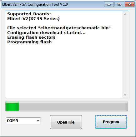
Now we can exit the Xilinx IDE and connect up the Elbert V2 Development board using a USB cable. Next load up the 'ElbertV2Config' program and choose the appropriate COM file for your Elbert V2 development board...mine is on COM5:


Click on the ' Open File' button and Navigate to the folder where the Nand gate project was stored. Locate the Binary file and select it:


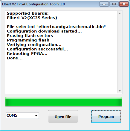
When ready click 'Program' and the FPGA will be programmed:


Once the programming has been completed the following will be displayed:


Now lets discuss NAND gate functions and what they do and how they work.  A NAND gate is a logic function created in electronics.  It is a shortened version of Not A and B.  It means that an input A and an input B are 'anded' together and then the output is inverted.  Information on Nand gates can be found here:


We have implemented an 8 input Nand Gate.  If we had to draw a symbol it would look like this:


The boolean function is:


The truth table for this function would be:


If we now look at the FPGA Development board and set the DIP switches appropriately we should see LED 8 light up:

If all of the switches are off - LED 8 is off:


But if any switch is ON then LED 8 lights up:


Here is a very short video showing the board in operation...no sound because there isn't much to say!


Thats all for now....take care - Langster