Here is a post on implementing a counter on the Numato Labs FPGA development board. I am still learning FPGA technology and thought it would be useful to share what has been achieved.
One of the most useful aspects of FPGA technology is the ability to choose which pins do what and being able to customize the function of the circuit with ease. Once it becomes apparent that this is possible and quite simple to achieve FPGAs become very attractive quite quickly.
In this tutorial I'm going to create a digital counter. Counters are used very often in digital electronics either to aid timing circuits and also to divide the frequency of clock signals to lower values.
Wikipedia Entry on digital counters
In the time before FPGA technology was available counters could be made by connecting several JK flip flop circuits together. It was also possible to buy counter circuits in TTL or CMOS integrated circuits. The difficulty with these circuits is that the number of bits present in the counters were fixed. With an FPGA any number of bits is possible - cool huh!
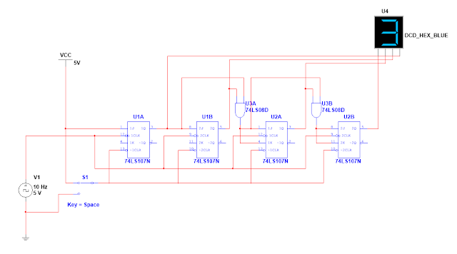 |
| A 4 bit Digital counter using TTL logic |
Lets implement a counter using the Mimas V2 FPGA development board! This can also be made to work with the Elbert V2 development board if required.
Fire up Xilinx WebISE and setup a new project for the Mimas V2 FPGA Board by selecting the following settings:
Click Ok when ready and then add a new source - select VHDL module and give the source a suitable name...
Click Next when ready...and then add the details shown below:
Click Next when ready to display the summary screen:
Click Finish when ready to return to the main screen...It should look similar to this:
The source has been added and the code is displayed. Comments are the statements preceded with '--' and in green text. I like to remove them unless the comment is useful, mostly I write my own comments. Comments are ignored during the 'compiling' process.
Here is the code without comments:
LIBRARY IEEE;
USE IEEE.STD_LOGIC_1164.ALL;
ENTITY LED_flasher IS
PORT (
clock_in : IN STD_LOGIC;
LED_out : OUT STD_LOGIC);
END LED_flasher;
ARCHITECTURE Behavioral OF LED_flasher IS
BEGIN
END Behavioral;
Lets discuss the code very quickly to explain what it does:
LIBRARY IEEE;
USE IEEE.STD_LOGIC_1164.ALL;
These two lines open the STD_LOGIC_1164 package of the IEEE library. They add useful functions and definitions similar to a library file in C.
ENTITY LED_flasher IS
PORT (
clock_in : IN STD_LOGIC;
LED_out : OUT STD_LOGIC);
END LED_flasher;
The entity statement is the section of the code where all the inputs and outputs are
defined. I like to think of it as the part of the code which describes what will happen. In this case there is an input called clock_in which will read a digital signal in from a pin and LED_out which will drive a pin as an output.
ARCHITECTURE Behavioral OF LED_flasher IS
BEGIN
END Behavioral;
The architecture statement is the section of the code that fetches the inputs, performs some processing and then displays the outputs. In this case we are going to write VHDL code in the architecture section which reads in the 100 MHz clock signal and then divides that down to a much lower frequency so that we can use the lower frequency signal to drive an LED. The method we are going to use to achieve this is to implement a counter - a section of code which will essentially count how many clock cycles have occurred and when the required number is reached, flash an LED!
A counter is a common method for reducing a 100 MHz clock down to a lower frequency - lets say a 1 Hz waveform. Why use a counter? Because a binary counter increments whenever the 100 MHz clock pulses and it goes through a transition sequence from 0 to 1 each time. We can use binary to represent this as counting as 0000, 0001, 0010, 0011, 0100, 0101, 0110, 0111...all the way up to 101111101011110000100000000(2) - 100,000,000(10)
If we look carefully it can be seen when the clock pulses that each bit of the count is half the value of the previous bit and that means that whilst counting the clock pulses the clock frequency is being divided by two. If we keep counting the clock pulses eventually we will divide the clock down to a frequency that can be seen by the human eye, we just need a counter with enough bits to do that.
Here is a useful page on counters if things are unclear:
What we need to do is calculate how many bits we need to divide 100 MHz down to 1 Hz. We know that if we had a 1 bit counter then the 100 MHz clock will be divided down to 50 MHz. If we have a 4 bit counter then the 100 MHz clock will be divided down to 12.5 MHz as:
100 MHz / 2 = 50 MHz....50 MHz / 2 = 25 MHz....25 MHz / 2 = 12.5 MHz etc
We could just perform all of the calculations and count how many times the division occurs...that tells us how many bits are required or...we can use binary representation of the decimal numbers and count how many bits we need!
100 000 000 is represented as 101 1111 0101 1110 0001 0000 0000(2) in binary. Lets count how many digits are present in the binary number as this tells us how many bits we will need. The binary number has 27 bits so a 27 bit counter is required in order to divide 100 MHz to 1 Hz....that is a lot of bits, its a good thing we don't have to build this with JK flip flops....27 flip flops to be powered and wired up and clocked would be months of work!
Lets plan to write the code - we need an If statement which counts how many clock pulses has occurred and then divide the count by two each time a clock pulse occurs and then repeat this process twenty seven times. We need this to happen when the clock pulse changes state from Low to High....here is the code for the architecture statement:
ARCHITECTURE Behavioral OF LED_flasher IS
SIGNAL counter : STD_LOGIC_VECTOR(27 DOWNTO 0);
BEGIN
PROCESS (clock_in) IS
BEGIN
IF rising_edge(clock_in) THEN
counter <= counter + 1;
END IF;
END PROCESS
LED_out <= counter(27);
END Behavioral;
Lets discuss how the code works...
SIGNAL counter : STD_LOGIC_VECTOR(27 DOWNTO 0);
The above line implements an internal 27 bit counter circuit in the FPGA. It is not passed to the any of the external pins at the moment so it will be completely invisible.
PROCESS (clock_in) IS
BEGIN
IF rising_edge(clock_in) THEN
counter <= counter + 1;
END IF;
END PROCESS
The process section is fairly self explanatory when the 100 MHz clock pulse goes from low to high the signal counter is incremented by one. Its almost exactly the same as an IF statement in C or C++.
LED_out <= counter(27);
The above line of code tells the output pin called LED_out to mirror the state of the 27th bit of the counter. When bit 27 of the counter is high then LED_out will be high. If we choose to connect this pin to an LED it will flash.
In order for this code to work an extra libary must be included:
USE IEEE.STD_LOGIC_UNSIGNED.ALL;
Here is the complete code - just in case it's required:
LIBRARY IEEE;
USE IEEE.STD_LOGIC_1164.ALL;
USE IEEE.STD_LOGIC_UNSIGNED.ALL;
ENTITY LED_flasher IS
PORT (
clock_in : IN STD_LOGIC;
LED_out : OUT STD_LOGIC
);
END LED_flasher;
ARCHITECTURE Behavioral OF LED_flasher IS
SIGNAL counter : STD_LOGIC_VECTOR(27 DOWNTO 0);
BEGIN
PROCESS (clock_in) IS
BEGIN
IF rising_edge(clock_in) THEN
counter <= counter + 1;
END IF;
END PROCESS;
LED_out <= counter(27);
END Behavioral;
At this point I would save the file...just in case! Here is what should be on screen:
To ensure all the code has been written correctly lets 'Synthesize' the code...right click on Synthesize - XST and select Run...
At the end of the process a green tick should appear and there should not be any warnings or error messages. If there are...there is a typing error somewhere in the code!
A useful tool with Xilinx WebISE is the ability to simulate the logic of how the code will behave. Just for fun lets do a simulation and see what happens. We could write an implementation constraints file here which tells the compiler which pins on the FPGA we want to be the inputs and outputs and it would perform something but we have no idea if our code will perform as intended. This is why its sometimes a good idea to simulate what the code will perform before we upload it to the FPGA.
In order to simulate the code, we need something to exercise the inputs and monitor the
outputs. This is known as a test bench in VHDL programming. It is basically another text file which tells the simulation program to exercise the inputs with suitable signals and then display the output - whatever that might be!
Lets add a new source to our project - select VHDL test bench and give it a sensible name:
Click Next when ready and then associate the test bench with the source code to be simulated:
Click Next when ready to display the summary screen:
Click finish when ready to return to the main project screen, helpfully Xilinx WebISE has generated a lot of code for us:
I like to remove the top comments...I don't find them useful. Here is the full code...just in case:
LIBRARY ieee;
USE ieee.std_logic_1164.ALL;
ENTITY LED_flasher_TB IS
END LED_flasher_TB;
ARCHITECTURE behavior OF LED_flasher_TB IS
COMPONENT LED_flasher
PORT (
clock_in : IN std_logic;
LED_out : OUT std_logic
);
END COMPONENT;
SIGNAL clock_in : std_logic := '0';
SIGNAL LED_out : std_logic;
CONSTANT clock_in_period : TIME := 10 ns;
BEGIN
uut : LED_flasher
PORT MAP(
clock_in => clock_in,
LED_out => LED_out
);
clock_in_process : PROCESS
BEGIN
clock_in <= '0';
WAIT FOR clock_in_period/2;
clock_in <= '1';
WAIT FOR clock_in_period/2;
END PROCESS;
stim_proc : PROCESS
BEGIN
WAIT FOR 100 ns;
WAIT FOR clock_in_period * 10;
WAIT;
END PROCESS;
END;
The above test bench code is quite similar to the actual VHDL code written before it has a component declaration, the same input process etc. The difference is however that the inputs are now being preset with values in order to assess what the output will do:
clock_in_process : PROCESS
BEGIN
clock_in <= '0';
WAIT FOR clock_in_period/2;
clock_in <= '1';
WAIT FOR clock_in_period/2;
END PROCESS;
The above section of test bench code simulates counter process - the clock_in signal is set to zero. the program then waits for half a clock period, the clock_in signal is set to one and then the program waits for another half clock period. This process will repeat forever...
As the LED_out pin does not do anything there is no extra code to write in the stim_proc section. Lets see the result:
Click on the ISIM simulation button and select the test bench file and then select run 'Simulate Behavioral Model':
Once complete a new window should appear which looks like this:
The screen shows the output of the simulation which ran for 1000 nano-seconds....not very long! We cannot see what happened at the output as not enough time passed. We can see that the clock_in signal changed state. If we click on the magnifier icon we will be able to see the clock signal more clearly:
Look - a red line and an 'X' - this means that there is an issue. The simulator cannot decide what state the LED_out pin should do. This is because the counter has been started in an unknown state. We need to modify the original VHDL code to initialise the counter in a zero state no matter what:
We need to change the line:
SIGNAL counter : STD_LOGIC_VECTOR(27 DOWNTO 0);
To this line:
SIGNAL counter : STD_LOGIC_VECTOR(27 DOWNTO 0) := (others=>'0');
Now save the code and then run synthesize again...and then re-run the simulate behavioral model...
This may take a while!
So the red line has disappeared...but the LED_out pin never changes state. In order to see if the code will work we need to run the simulation for a longer time period. The issue is that it will take a long time to process all of that data - the simulation program has to run the code in order to simulate the results...Change the simulation time to 2.5 seconds and prepare to wait:
Once the simulation has completed this what should be displayed:
The LED_out pin is changing state which means everything worked! Lets get on with the real thing!
Click on the View radio button and then select 'add new source':
On the screen that appears select implementation constraints file and then choose a suitable file name:
Click Next to display the summary screen:
Click finish to return to the main screen.
The method of choosing which pins are connected to the FPGA are decided by the implementation constraints file. In theory any pins could be used to read in the input and any pins could be used for an output. In practice because a development board is being used the pin connected to the clock crystal must be selected for the clock_in signal and a pin connected to an LED must be used for the LED_out signal.
Here is the code:
#++++++++++++++++++++++++++++++++++++++++++++++++++++++++++++++++++++++++++++++++#
# This file is a .ucf for Mimas V2 #
# To use it in your project : #
# * Remove or comment the lines corresponding to unused pins in the project #
# * Rename the used signals according to the your project #
#++++++++++++++++++++++++++++++++++++++++++++++++++++++++++++++++++++++++++++++++#
CONFIG VCCAUX = "3.3" ;
NET "clock_in" LOC = V10 | IOSTANDARD = LVCMOS33 | PERIOD = 100MHz;
###################################################################################
# LEDs #
###################################################################################
NET "LED_out" LOC = P15 | IOSTANDARD = LVCMOS33 | DRIVE = 8 | SLEW = FAST;
The UCF code is fairly simple to understand....the 100 MHz clock crystal is connected to pin V10. So we tell the compiler to connect the internal signal called clock_in to pin V10. The first LED physical LED is connected to pin P15 so connect the internal signal called LED_out to pin P15.
Save the code and then click on the green arrow to implement the top module - compile all the code!
If everything went according to plan there should be green ticks next to Synthesize XST and Implement Design:
Right click on Generate program file and select process properties and then select create binary configuration file:
Click Ok and then select 'Generate Programming File':
Once that is complete - connect up the Mimas V2 Development board to a suitable USB port and then load up the Mimas V2 programming tool:
Once complete the LED on position zero should flash every once a second!
Here is a video showing my board in action!
Next post will discuss generating multiple divided clock signals. Take care - Langster!


