Sunday 17 September 2017

Pulse Oximeter Functionality for a Medical Device

It has again been some time since I did any work on the medical device I have been developing, I've as usual, been busy!  The previous post is here in case it is of interest:

http://langster1980.blogspot.co.uk/2017/06/myoware-muscle-sensor-circuits-from.html

The gentlemen for whom I'm developing this hardware for has requested some additional functionality. The additional functionality requested is a Pulse Oximetry measurement.  Pulse Oximetry is the measurement of a person's pulse along with how much oxygen is present within their blood.  It is a common measurement made by medical practitioners to ensure their patients are in good health.  I suspect for the medical device, this information will be correlated with a person's breathing to assess how well a person's lungs are working and how much oxygen from the air is getting into their blood.

Image by Nonin Medical - http://www.nonin.com/What-is-Pulse-Oximetry
Here is an article by Nonin Medical on Pulse Oximetry:

http://www.nonin.com/What-is-Pulse-Oximetry

Here is the wikipedia article on Pulse Oximetry:

https://en.wikipedia.org/wiki/Pulse_oximetry

Here is another article on Pulse Oximetry:

https://www.howequipmentworks.com/pulse_oximeter/

The measurement works by shining a bright light through the a suitable point on the patient's skin and detecting the diffused light and from that the pulse and oxygen levels can be calculated.  The units used are SPO2 which stands for Peripheral Oxygen Saturation where:

SP = Peripheral saturation
O2 = Chemical symbol for an Oxygen molecule

There is a formula associated with Pulse Oximetry:


Where HbO2 is Oxygenated Haemoglobin and Hb is Deoxygenated Haemoglobin*

SPO2 is presented as a percentage and most people in normal conditions exhibit 94 to 99% saturation of oxygen in their blood.  If a person were unwell due to breathing difficulty then their SPO2 is lower.  If a person's SPOis below 65% then their ability to think clearly is impaired and if below 55% most people have lost consciousness.

*Haemoglobin is the red coloured metallo-protein within human blood which contains iron and carries oxygen around the body.

So that is the theory!  Lets talk about how one might design an electronic circuit to measure a person's SPO2 level.  We need to shine a light through an exposed part of the patient's skin say on the top of their index finger and measure the amount of light present at the bottom of the finger after the light has travelled through their skin.  At the same time the light signal needs to be converted to an electrical signal and then filtered.  It then will probably need to be amplified and finally converted from an analogue signal to a digital signal for processing by a microcontroller and finally displaying the resulting measurement.

It is not a particularly difficult circuit to design and plenty of other people have already done so.  I have put some of the sites I used as research below for interest:

https://www.swharden.com/wp/2013-04-14-simple-diy-ecg-pulse-oximeter-version-2/

http://www.instructables.com/id/Simple-DIY-Pulse-Sensor/

http://www.elektroda.pl/rtvforum/topic1655378.html?l=en

I may yet design my own implementation as it could be one way to reduce costs.  There is an Arduino R3 shield available though and it's open source.  It is made by ProtoCentral and is called the Proto Central AFE4490 Pulse Oximeter Shield V2.  It cost £71.12 which I actually think is a bit expensive however it does look to be well designed and implemented.

Image Credit - ProtoCentral AFE4490 Pulse Oximeter Shield for Arduino - v2
It can be bought from their website below:

Pulse Oximeter Arduino Shield

Because the device is completely open source (Very cool - I whole heartedly approve) the schematic is below:
The whole circuit is based around a very clever integrated circuit by Texas Instruments - the
AFE4490. The datasheet for this device is here:

http://www.ti.com/lit/ds/sbas602h/sbas602h.pdf

Basically the optical signal from the supplied finger clip connects to the nine way 'D type' connector on the Arduino shield. The signal output is protected from being too high by the the circuit labelled 'Protection circuit'  The diodes ensure that the electrical signals passed to and from the clip can never be greater than 3.3 Vdc which ensures that no damage can occur.

The analogue signal sent from the clip is processed by the AD4490 device which is a complete analogue front end device for pulse oximetry.  The device provides the electrical signals to drive the sensor clip, a 22 bit analogue to digital converter to change the analogue signal output from the sensor to a form which can be easily read into a microcontroller using the Serial Peripheral Interface (SPI) protocol.

The next part of the circuit is a simple power supply regulator from 5 Vdc to 3.3 Vdc with some filtering to prevent electronic noise from the Arduino R3 affecting the measurement circuitry.

A logic level converter device is present to ensure that the 3.3 Vdc signals from the AD4490 device are turned into 5 Vdc so that they are correctly read into the arduino and processed appropriately. There are two FET logic level converter circuits present to convert the 3.3 Vdc LED diagnostic signals to 5 Vdc for processing by the Arduino.

The final section shows how all the connections on the Shield connect to the Arduino R3.

The circuit looks to be exactly how one would use the AD4490 having read the datasheet in it's entirety.  Reading and understanding or interpreting datasheets is a true skill needed for aspiring electronics design engineers.

ProtoCentral have very helpfully provided example code which can be downloaded from their github site:

https://github.com/Protocentral/AFE4490_Oximeter/tree/master/arduino

I've uploaded the text only code to my arduino R3.

Lets see the circuit in action!


Here is the serial output:


Well there we have it - I'm alive, my blood is well oxygenated and my heart is beating normally! Each measurement is taken once a second and if the clip is removed an error is reported.

I modified the code a little so that I can use the excellent telemetry viewer Java applet to graph the output:

http://farrellf.com/TelemetryViewer/

Here is the modified Arduino code in case it's needed:

 //////////////////////////////////////////////////////////////////////////////////////////  
 //  
 //  AFE44xx Arduino Firmware  
 //  
 //  Copyright (c) 2016 ProtoCentral  
 //    
 //  SpO2 computation based on original code from Maxim Integrated   
 //  
 //  This software is licensed under the MIT License(http://opensource.org/licenses/MIT).   
 //    
 //  THE SOFTWARE IS PROVIDED "AS IS", WITHOUT WARRANTY OF ANY KIND, EXPRESS OR IMPLIED, INCLUDING BUT   
 //  NOT LIMITED TO THE WARRANTIES OF MERCHANTABILITY, FITNESS FOR A PARTICULAR PURPOSE AND NONINFRINGEMENT.   
 //  IN NO EVENT SHALL THE AUTHORS OR COPYRIGHT HOLDERS BE LIABLE FOR ANY CLAIM, DAMAGES OR OTHER LIABILITY,   
 //  WHETHER IN AN ACTION OF CONTRACT, TORT OR OTHERWISE, ARISING FROM, OUT OF OR IN CONNECTION WITH THE   
 //  SOFTWARE OR THE USE OR OTHER DEALINGS IN THE SOFTWARE.  
 //  
 //  For information on how to use the HealthyPi, visit https://github.com/Protocentral/afe44xx_Oximeter  
 /////////////////////////////////////////////////////////////////////////////////////////  
 #include <string.h>  
 #include <SPI.h>  
 #include <math.h>  
 //afe44xx Register definition  
 #define CONTROL0  0x00  
 #define LED2STC   0x01  
 #define LED2ENDC  0x02  
 #define LED2LEDSTC  0x03  
 #define LED2LEDENDC  0x04  
 #define ALED2STC  0x05  
 #define ALED2ENDC  0x06  
 #define LED1STC   0x07  
 #define LED1ENDC  0x08  
 #define LED1LEDSTC  0x09  
 #define LED1LEDENDC  0x0a  
 #define ALED1STC  0x0b  
 #define ALED1ENDC  0x0c  
 #define LED2CONVST  0x0d  
 #define LED2CONVEND  0x0e  
 #define ALED2CONVST  0x0f  
 #define ALED2CONVEND 0x10  
 #define LED1CONVST  0x11  
 #define LED1CONVEND  0x12  
 #define ALED1CONVST  0x13  
 #define ALED1CONVEND 0x14  
 #define ADCRSTCNT0  0x15  
 #define ADCRSTENDCT0 0x16  
 #define ADCRSTCNT1  0x17  
 #define ADCRSTENDCT1 0x18  
 #define ADCRSTCNT2  0x19  
 #define ADCRSTENDCT2 0x1a  
 #define ADCRSTCNT3  0x1b  
 #define ADCRSTENDCT3 0x1c  
 #define PRPCOUNT  0x1d  
 #define CONTROL1  0x1e  
 #define SPARE1   0x1f  
 #define TIAGAIN   0x20  
 #define TIA_AMB_GAIN 0x21  
 #define LEDCNTRL  0x22  
 #define CONTROL2  0x23  
 #define SPARE2   0x24  
 #define SPARE3   0x25  
 #define SPARE4   0x26  
 #define SPARE4   0x26  
 #define RESERVED1  0x27  
 #define RESERVED2  0x28  
 #define ALARM   0x29  
 #define LED2VAL   0x2a  
 #define ALED2VAL  0x2b  
 #define LED1VAL   0x2c  
 #define ALED1VAL  0x2d  
 #define LED2ABSVAL  0x2e  
 #define LED1ABSVAL  0x2f  
 #define DIAG   0x30  
 #define count 60  
 #define CES_CMDIF_PKT_START_1  0x0A  
 #define CES_CMDIF_PKT_START_2  0xFA  
 #define CES_CMDIF_TYPE_DATA  0x02  
 #define CES_CMDIF_PKT_STOP  0x0B  
 //int IRheartsignal[count];  
 //int Redheartsignal[count];  
 int IRdc[count];  
 int Reddc[count];  
 double difIRheartsig_dc;  
 double difREDheartsig_dc;  
 double powdifIR;  
 double powdifRed;  
 double IRac;   
 double Redac;  
 double SpOpercentage;  
 double Ratio;  
 const int SPISTE = 7; // chip select  
 const int SPIDRDY = 2; // data ready pin   
 volatile int drdy_trigger = LOW;  
 void afe44xxInit (void);  
 void afe44xxWrite (uint8_t address, uint32_t data);  
 uint32_t afe44xxRead (uint8_t address);  
 signed long average_BPM( signed long );  
 volatile char DataPacketHeader[6];  
 volatile char DataPacket[10];  
 volatile char DataPacketFooter[2];  
 int datalen = 0x09;  
 unsigned long time;  
 volatile static int SPI_RX_Buff_Count = 0;  
 volatile char *SPI_RX_Buff_Ptr;  
 volatile int afe44xx_data_ready = false;  
 volatile unsigned int pckt =0, buff=0,t=0;  
 unsigned long ueegtemp = 0, ueegtemp2 = 0;  
 unsigned long IRtemp,REDtemp;  
 signed long seegtemp=0, seegtemp2=0;  
 volatile int i;  
 uint16_t aun_ir_buffer[100]; //infrared LED sensor data  
 uint16_t aun_red_buffer[100]; //red LED sensor data  
 #define FS      25  //sampling frequency  
 #define BUFFER_SIZE (FS*4)   
 #define MA4_SIZE 4 // DONOT CHANGE  
 #define min(x,y) ((x) < (y) ? (x) : (y))  
 const uint8_t uch_spo2_table[184]={ 95, 95, 95, 96, 96, 96, 97, 97, 97, 97, 97, 98, 98, 98, 98, 98, 99, 99, 99, 99,   
        99, 99, 99, 99, 100, 100, 100, 100, 100, 100, 100, 100, 100, 100, 100, 100, 100, 100, 100, 100,   
        100, 100, 100, 100, 99, 99, 99, 99, 99, 99, 99, 99, 98, 98, 98, 98, 98, 98, 97, 97,   
        97, 97, 96, 96, 96, 96, 95, 95, 95, 94, 94, 94, 93, 93, 93, 92, 92, 92, 91, 91,   
        90, 90, 89, 89, 89, 88, 88, 87, 87, 86, 86, 85, 85, 84, 84, 83, 82, 82, 81, 81,   
        80, 80, 79, 78, 78, 77, 76, 76, 75, 74, 74, 73, 72, 72, 71, 70, 69, 69, 68, 67,   
        66, 66, 65, 64, 63, 62, 62, 61, 60, 59, 58, 57, 56, 56, 55, 54, 53, 52, 51, 50,   
        49, 48, 47, 46, 45, 44, 43, 42, 41, 40, 39, 38, 37, 36, 35, 34, 33, 31, 30, 29,   
        28, 27, 26, 25, 23, 22, 21, 20, 19, 17, 16, 15, 14, 12, 11, 10, 9, 7, 6, 5,   
        3, 2, 1 } ;  
 static int32_t an_x[ BUFFER_SIZE];   
 static int32_t an_y[ BUFFER_SIZE];   
 volatile int8_t n_buffer_count; //data length  
 int32_t n_spo2; //SPO2 value  
 int8_t ch_spo2_valid; //indicator to show if the SPO2 calculation is valid  
 int32_t n_heart_rate; //heart rate value  
 int8_t ch_hr_valid; //indicator to show if the heart rate calculation is valid  
 long status_byte=0;  
 uint8_t LeadStatus=0;  
 boolean leadoff_deteted = true;  
 uint8_t spo2_probe_open = false;  
 int dec=0;  
 void setup()  
 {  
   Serial.begin(57600);  
   Serial.println("Initialising AFE44xx.. ");    
   delay(2000) ;  // pause for a moment  
   SPI.begin();   
   // set the directions  
   pinMode (SPISTE,OUTPUT);//Slave Select  
   pinMode (SPIDRDY,INPUT);// data ready   
   attachInterrupt(0, afe44xx_drdy_event, RISING ); // Digital2 is attached to Data ready pin of AFE is interrupt0 in ARduino  
   // set SPI transmission  
   SPI.setClockDivider (SPI_CLOCK_DIV8); // set Speed as 2MHz , 16MHz/ClockDiv  
   SPI.setDataMode (SPI_MODE0);     //Set SPI mode as 0  
   SPI.setBitOrder (MSBFIRST);      //MSB first  
 // Packet structure  
  DataPacketHeader[0] = CES_CMDIF_PKT_START_1; //packet header1 0x0A  
  DataPacketHeader[1] = CES_CMDIF_PKT_START_2; //packet header2 0xFA  
  DataPacketHeader[2] = datalen;        // data length 9  
  DataPacketHeader[3] = (uint8_t)(datalen >> 8);  
  DataPacketHeader[4] = CES_CMDIF_TYPE_DATA;  
  DataPacketFooter[0] = 0x00;  
  DataPacketFooter[1] = CES_CMDIF_PKT_STOP;  
   afe44xxInit ();   
   Serial.println("Initialisation Complete!");  
 }  
 /////////////////////////////////////////////////////////////////////////////////////////////////////////////////  
 void loop()  
 {    
    if (drdy_trigger == HIGH)   
    {  
     detachInterrupt(0);  
     afe44xxWrite(CONTROL0,0x000001);   
     IRtemp = afe44xxRead(LED1VAL);  
     afe44xxWrite(CONTROL0,0x000001);   
     REDtemp = afe44xxRead(LED2VAL);    
     afe44xx_data_ready = true;  
    }   
  if(afe44xx_data_ready == true)  
  {  
    IRtemp = (unsigned long) (IRtemp<<10);  
    seegtemp = (signed long) (IRtemp);  
    seegtemp = (signed long) (seegtemp>>10);   
    REDtemp = (unsigned long) (REDtemp<<10);  
    seegtemp2 = (signed long) (REDtemp);  
    seegtemp2 = (signed long) (seegtemp2>>10);  
    if(dec==20)  
    {  
     aun_ir_buffer[n_buffer_count]=(uint16_t) (seegtemp>>4);  
     aun_red_buffer[n_buffer_count]=(uint16_t) (seegtemp2>>4);  
     n_buffer_count++;  
     dec=0;  
    }  
    dec++;  
    if(n_buffer_count>99)  
    {  
     estimate_spo2(aun_ir_buffer, 100, aun_red_buffer, &n_spo2, &ch_spo2_valid,&n_heart_rate, &ch_hr_valid);   
     if(n_spo2 == -999)  
      Serial.println("Probe error!!!!");  
     else  
     {   
       // removed by AL to allow live graphing by telemetry viewer  
       //Serial.print("calculating sp02...");  
       //Serial.print(" Sp02 : ");  
       //Serial.print(n_spo2);  
       //Serial.print("% ,");   
       //Serial.print("Pulse rate :");  
       //Serial.print(n_heart_rate);              
       //Serial.println(" bpm");  
       Serial.print("SP02 (%), Pulse Rate (BPM)");  
       Serial.print(n_spo2);  
       Serial.print(",");  
       Serial.print(n_heart_rate);  
       Serial.print(",");  
       Serial.println();  
     }  
     n_buffer_count=0;  
    }       
    afe44xx_data_ready = false;  
    drdy_trigger = LOW;  
    attachInterrupt(0, afe44xx_drdy_event, RISING );     
  }            
 }  
 ///////// Gets Fired on DRDY event/////////////////////////////  
 void afe44xx_drdy_event()  
 {  
  drdy_trigger = HIGH;  
 }  
 ////////////////AFE44xx initialization//////////////////////////////////////////  
 void afe44xxInit (void)  
 {   
  // Serial.println("afe44xx Initialization Starts");   
    afe44xxWrite(CONTROL0,0x000000);  
    afe44xxWrite(CONTROL0,0x000008);   
    afe44xxWrite(TIAGAIN,0x000000); // CF = 5pF, RF = 500kR  
    afe44xxWrite(TIA_AMB_GAIN,0x000001);   
    afe44xxWrite(LEDCNTRL,0x001414);    
    afe44xxWrite(CONTROL2,0x000000); // LED_RANGE=100mA, LED=50mA   
    afe44xxWrite(CONTROL1,0x010707); // Timers ON, average 3 samples   
    afe44xxWrite(PRPCOUNT, 0X001F3F);  
   afe44xxWrite(LED2STC, 0X001770);   
   afe44xxWrite(LED2ENDC,0X001F3E);   
   afe44xxWrite(LED2LEDSTC,0X001770);  
   afe44xxWrite(LED2LEDENDC,0X001F3F);  
   afe44xxWrite(ALED2STC, 0X000000);   
   afe44xxWrite(ALED2ENDC, 0X0007CE);  
   afe44xxWrite(LED2CONVST,0X000002);   
   afe44xxWrite(LED2CONVEND, 0X0007CF);  
   afe44xxWrite(ALED2CONVST, 0X0007D2);   
   afe44xxWrite(ALED2CONVEND,0X000F9F);   
   afe44xxWrite(LED1STC, 0X0007D0);   
   afe44xxWrite(LED1ENDC, 0X000F9E);  
   afe44xxWrite(LED1LEDSTC, 0X0007D0);  
   afe44xxWrite(LED1LEDENDC, 0X000F9F);  
   afe44xxWrite(ALED1STC, 0X000FA0);   
   afe44xxWrite(ALED1ENDC, 0X00176E);  
   afe44xxWrite(LED1CONVST, 0X000FA2);  
   afe44xxWrite(LED1CONVEND, 0X00176F);   
   afe44xxWrite(ALED1CONVST, 0X001772);   
   afe44xxWrite(ALED1CONVEND, 0X001F3F);  
   afe44xxWrite(ADCRSTCNT0, 0X000000);  
   afe44xxWrite(ADCRSTENDCT0,0X000000);   
   afe44xxWrite(ADCRSTCNT1, 0X0007D0);   
   afe44xxWrite(ADCRSTENDCT1, 0X0007D0);  
   afe44xxWrite(ADCRSTCNT2, 0X000FA0);  
   afe44xxWrite(ADCRSTENDCT2, 0X000FA0);   
   afe44xxWrite(ADCRSTCNT3, 0X001770);   
   afe44xxWrite(ADCRSTENDCT3, 0X001770);  
   delay(1000);  
   // Serial.println("afe44xx Initialization Done");   
 }  
 /////////////////////////////////////////////////////////////////////////////////////////////////////////////////  
 void afe44xxWrite (uint8_t address, uint32_t data)  
 {  
   digitalWrite (SPISTE, LOW); // enable device  
   SPI.transfer (address); // send address to device  
   SPI.transfer ((data >> 16) & 0xFF); // write top 8 bits  
   SPI.transfer ((data >> 8) & 0xFF); // write middle 8 bits  
   SPI.transfer (data & 0xFF); // write bottom 8 bits    
   digitalWrite (SPISTE, HIGH); // disable device  
 }  
 /////////////////////////////////////////////////////////////////////////////////////////////////////////////////  
 unsigned long afe44xxRead (uint8_t address)  
 {      
   unsigned long data=0;  
   digitalWrite (SPISTE, LOW); // enable device  
   SPI.transfer (address); // send address to device  
   //SPI.transfer (data);  
   data |= ((unsigned long)SPI.transfer (0)<<16); // read top 8 bits data  
   data |= ((unsigned long)SPI.transfer (0)<<8); // read middle 8 bits data  
   data |= SPI.transfer (0); // read bottom 8 bits data  
   digitalWrite (SPISTE, HIGH); // disable device  
   return data; // return with 24 bits of read data  
 }  
 /////////////////////////////////////////////////////////////////////////////////////////////////////////////////  
 void estimate_spo2(uint16_t *pun_ir_buffer, int32_t n_ir_buffer_length, uint16_t *pun_red_buffer, int32_t *pn_spo2, int8_t *pch_spo2_valid, int32_t *pn_heart_rate, int8_t *pch_hr_valid)  
 {  
  uint32_t un_ir_mean,un_only_once ;  
  int32_t k, n_i_ratio_count;  
  int32_t i, s, m, n_exact_ir_valley_locs_count, n_middle_idx;  
  int32_t n_th1, n_npks, n_c_min;    
  int32_t an_ir_valley_locs[15] ;  
  int32_t n_peak_interval_sum;  
  int32_t n_y_ac, n_x_ac;  
  int32_t n_spo2_calc;   
  int32_t n_y_dc_max, n_x_dc_max;   
  int32_t n_y_dc_max_idx, n_x_dc_max_idx;   
  int32_t an_ratio[5], n_ratio_average;   
  int32_t n_nume, n_denom ;  
  // calculates DC mean and subtract DC from ir  
  un_ir_mean =0;   
  for (k=0 ; k<n_ir_buffer_length ; k++ ) un_ir_mean += pun_ir_buffer[k] ;  
  un_ir_mean =un_ir_mean/n_ir_buffer_length ;  
  // remove DC and invert signal so that we can use peak detector as valley detector  
  for (k=0 ; k<n_ir_buffer_length ; k++ )   
   an_x[k] = -1*(pun_ir_buffer[k] - un_ir_mean) ;   
  // 4 pt Moving Average  
  for(k=0; k< BUFFER_SIZE-MA4_SIZE; k++){  
   an_x[k]=( an_x[k]+an_x[k+1]+ an_x[k+2]+ an_x[k+3])/(int)4;      
  }  
  // calculate threshold   
  n_th1=0;   
  for ( k=0 ; k<BUFFER_SIZE ;k++){  
   n_th1 += an_x[k];  
  }  
  n_th1= n_th1/ ( BUFFER_SIZE);  
  if( n_th1<30) n_th1=30; // min allowed  
  if( n_th1>60) n_th1=60; // max allowed  
  for ( k=0 ; k<15;k++) an_ir_valley_locs[k]=0;  
  // since we flipped signal, we use peak detector as valley detector  
  find_peak( an_ir_valley_locs, &n_npks, an_x, BUFFER_SIZE, n_th1, 4, 15 );//peak_height, peak_distance, max_num_peaks   
  n_peak_interval_sum =0;  
  if (n_npks>=2){  
   for (k=1; k<n_npks; k++) n_peak_interval_sum += (an_ir_valley_locs[k] -an_ir_valley_locs[k -1] ) ;  
   n_peak_interval_sum =n_peak_interval_sum/(n_npks-1);  
   *pn_heart_rate =(int32_t)( (FS*60)/ n_peak_interval_sum );  
   *pch_hr_valid = 1;  
  }  
  else {   
   *pn_heart_rate = -999; // unable to calculate because # of peaks are too small  
   *pch_hr_valid = 0;  
  }  
  // load raw value again for SPO2 calculation : RED(=y) and IR(=X)  
  for (k=0 ; k<n_ir_buffer_length ; k++ ) {  
    an_x[k] = pun_ir_buffer[k] ;   
    an_y[k] = pun_red_buffer[k] ;   
  }  
  // find precise min near an_ir_valley_locs  
  n_exact_ir_valley_locs_count =n_npks;   
  //using exact_ir_valley_locs , find ir-red DC andir-red AC for SPO2 calibration an_ratio  
  //finding AC/DC maximum of raw  
  n_ratio_average =0;   
  n_i_ratio_count = 0;   
  for(k=0; k< 5; k++) an_ratio[k]=0;  
  for (k=0; k< n_exact_ir_valley_locs_count; k++){  
   if (an_ir_valley_locs[k] > BUFFER_SIZE ){  
    *pn_spo2 = -999 ; // do not use SPO2 since valley loc is out of range  
    *pch_spo2_valid = 0;   
    return;  
   }  
  }  
  // find max between two valley locations   
  // and use an_ratio betwen AC compoent of Ir & Red and DC compoent of Ir & Red for SPO2   
  for (k=0; k< n_exact_ir_valley_locs_count-1; k++){  
   n_y_dc_max= -16777216 ;   
   n_x_dc_max= -16777216;   
   if (an_ir_valley_locs[k+1]-an_ir_valley_locs[k] >3){  
     for (i=an_ir_valley_locs[k]; i< an_ir_valley_locs[k+1]; i++){  
      if (an_x[i]> n_x_dc_max) {n_x_dc_max =an_x[i]; n_x_dc_max_idx=i;}  
      if (an_y[i]> n_y_dc_max) {n_y_dc_max =an_y[i]; n_y_dc_max_idx=i;}  
    }  
    n_y_ac= (an_y[an_ir_valley_locs[k+1]] - an_y[an_ir_valley_locs[k] ] )*(n_y_dc_max_idx -an_ir_valley_locs[k]); //red  
    n_y_ac= an_y[an_ir_valley_locs[k]] + n_y_ac/ (an_ir_valley_locs[k+1] - an_ir_valley_locs[k]) ;   
    n_y_ac= an_y[n_y_dc_max_idx] - n_y_ac;  // subracting linear DC compoenents from raw   
    n_x_ac= (an_x[an_ir_valley_locs[k+1]] - an_x[an_ir_valley_locs[k] ] )*(n_x_dc_max_idx -an_ir_valley_locs[k]); // ir  
    n_x_ac= an_x[an_ir_valley_locs[k]] + n_x_ac/ (an_ir_valley_locs[k+1] - an_ir_valley_locs[k]);   
    n_x_ac= an_x[n_y_dc_max_idx] - n_x_ac;   // subracting linear DC compoenents from raw   
    n_nume=( n_y_ac *n_x_dc_max)>>7 ; //prepare X100 to preserve floating value  
    n_denom= ( n_x_ac *n_y_dc_max)>>7;  
    if (n_denom>0 && n_i_ratio_count <5 && n_nume != 0)  
    {    
     an_ratio[n_i_ratio_count]= (n_nume*100)/n_denom ; //formular is ( n_y_ac *n_x_dc_max) / ( n_x_ac *n_y_dc_max) ;  
     n_i_ratio_count++;  
    }  
   }  
  }  
  // choose median value since PPG signal may varies from beat to beat  
  sort_ascend(an_ratio, n_i_ratio_count);  
  n_middle_idx= n_i_ratio_count/2;  
  if (n_middle_idx >1)  
   n_ratio_average =( an_ratio[n_middle_idx-1] +an_ratio[n_middle_idx])/2; // use median  
  else  
   n_ratio_average = an_ratio[n_middle_idx ];  
  if( n_ratio_average>2 && n_ratio_average <184){  
   n_spo2_calc= uch_spo2_table[n_ratio_average] ;  
   *pn_spo2 = n_spo2_calc ;  
   *pch_spo2_valid = 1;// float_SPO2 = -45.060*n_ratio_average* n_ratio_average/10000 + 30.354 *n_ratio_average/100 + 94.845 ; // for comparison with table  
  }  
  else{  
   *pn_spo2 = -999 ; // do not use SPO2 since signal an_ratio is out of range  
   *pch_spo2_valid = 0;   
  }  
 }  
 /////////////////////////////////////////////////////////////////////////////////////////////////////////////////  
 void find_peak( int32_t *pn_locs, int32_t *n_npks, int32_t *pn_x, int32_t n_size, int32_t n_min_height, int32_t n_min_distance, int32_t n_max_num )  
 /**  
 * \brief    Find peaks  
 * \par     Details  
 *        Find at most MAX_NUM peaks above MIN_HEIGHT separated by at least MIN_DISTANCE  
 *  
 * \retval    None  
 */  
 {  
   find_peak_above( pn_locs, n_npks, pn_x, n_size, n_min_height );  
   remove_close_peaks( pn_locs, n_npks, pn_x, n_min_distance );  
   *n_npks = min( *n_npks, n_max_num );  
 }  
 /////////////////////////////////////////////////////////////////////////////////////////////////////////////////  
 void find_peak_above( int32_t *pn_locs, int32_t *n_npks, int32_t *pn_x, int32_t n_size, int32_t n_min_height )  
 /**  
 * \brief    Find peaks above n_min_height  
 * \par     Details  
 *        Find all peaks above MIN_HEIGHT  
 *  
 * \retval    None  
 */  
 {  
  int32_t i = 1, n_width;  
  *n_npks = 0;  
  while (i < n_size-1){  
   if (pn_x[i] > n_min_height && pn_x[i] > pn_x[i-1]){   // find left edge of potential peaks  
    n_width = 1;  
    while (i+n_width < n_size && pn_x[i] == pn_x[i+n_width]) // find flat peaks  
     n_width++;  
    if (pn_x[i] > pn_x[i+n_width] && (*n_npks) < 15 ){   // find right edge of peaks  
     pn_locs[(*n_npks)++] = i;    
     // for flat peaks, peak location is left edge  
     i += n_width+1;  
    }  
    else  
     i += n_width;  
   }  
   else  
    i++;  
   // Serial.println("beat");  
  }  
 }  
 /////////////////////////////////////////////////////////////////////////////////////////////////////////////////  
 void remove_close_peaks(int32_t *pn_locs, int32_t *pn_npks, int32_t *pn_x, int32_t n_min_distance)  
 /**  
 * \brief    Remove peaks  
 * \par     Details  
 *        Remove peaks separated by less than MIN_DISTANCE  
 *  
 * \retval    None  
 */  
 {  
  int32_t i, j, n_old_npks, n_dist;  
  /* Order peaks from large to small */  
  sort_indices_descend( pn_x, pn_locs, *pn_npks );  
  for ( i = -1; i < *pn_npks; i++ ){  
   n_old_npks = *pn_npks;  
   *pn_npks = i+1;  
   for ( j = i+1; j < n_old_npks; j++ ){  
    n_dist = pn_locs[j] - ( i == -1 ? -1 : pn_locs[i] ); // lag-zero peak of autocorr is at index -1  
    if ( n_dist > n_min_distance || n_dist < -n_min_distance )  
     pn_locs[(*pn_npks)++] = pn_locs[j];  
   }  
  }  
  // Resort indices int32_to ascending order  
  sort_ascend( pn_locs, *pn_npks );  
 }  
 /////////////////////////////////////////////////////////////////////////////////////////////////////////////////  
 void sort_ascend(int32_t *pn_x, int32_t n_size)   
 /**  
 * \brief    Sort array  
 * \par     Details  
 *        Sort array in ascending order (insertion sort algorithm)  
 *  
 * \retval    None  
 */  
 {  
  int32_t i, j, n_temp;  
  for (i = 1; i < n_size; i++) {  
   n_temp = pn_x[i];  
   for (j = i; j > 0 && n_temp < pn_x[j-1]; j--)  
     pn_x[j] = pn_x[j-1];  
   pn_x[j] = n_temp;  
  }  
 }  
 /////////////////////////////////////////////////////////////////////////////////////////////////////////////////  
 void sort_indices_descend( int32_t *pn_x, int32_t *pn_indx, int32_t n_size)  
 /**  
 * \brief    Sort indices  
 * \par     Details  
 *        Sort indices according to descending order (insertion sort algorithm)  
 *  
 * \retval    None  
 */   
 {  
  int32_t i, j, n_temp;  
  for (i = 1; i < n_size; i++) {  
   n_temp = pn_indx[i];  
   for (j = i; j > 0 && pn_x[n_temp] > pn_x[pn_indx[j-1]]; j--)  
    pn_indx[j] = pn_indx[j-1];  
   pn_indx[j] = n_temp;  
  }  
 }  

Here is the output from Telemetry Viewer 0.4:


I think this is actually a very well implemented product and if I can use it as part of my project it will save me months of development...my only concern is cost and that it updates slowly and it also uses most of the program memory available on an ATMEL 328P Microcontroller.  One final comment I might make is that the example code provided is very long and complex.  It would be better if the initialisation functions and the measurement calculation functions were moved to a library.  It will make reading and writing code much simpler.

Whether I use this arduino shield or not is up for debate...I will probably discuss things further and come to a decision later.

Well that's all for now - Langster!

Tuesday 12 September 2017

Using Components in VHDL

Recently I was asked to provide a bit of assistance with some VHDL code - One of the blog readers was looking to implement a logic based CPU on the Mimas V2 Development board. I don't claim to be an expert in VHDL but the crux of his issue was using pre-written code in one project several times. The beauty of FPGA technology is that as long as there is space within the device and pins available it is possible to have as many logic functions as one wants!

There comes a point in FPGA programming where trying to put all of the code in one single source file becomes really awkward. The file would become very long to read and debug and it may make more sense to take a modular approach and re-use code from previous designs. Luckily for the FPGA design engineer it is possible to write and design modules in VHDL very easily and each module can be tested and used on it's own.

The way to implement this is to use the component keyword in VHDL and 'instantiate' as many of the modules or blocks of code as one wants.

In previous posts I have already used this method but I haven't really ever discussed it explicitly so here goes:
In a VHDL source module the code is organised into section statements known as:
  • Entities - The statement which defines the external input and output connections of the module.
  • Architectures - This is the code section which actually tells or defines the function of the module.
  • Components - A statement within the architecture section which allows the designer to link internal signals or external signals with pre-written VHDL code in another module.
  • Instances - A statement which actually creates the 'instance' of the external module code within another module. A designer can have multiple instances of a module within a design with one component statement as long as all of the connections are correctly port mapped.
Here is an example of an Entity statement:

entity EntitySection is
           Port ( clkinput : in STD_LOGIC;
                  input1 : in STD_LOGIC;
                  input2 : in STD_LOGIC;
                  input3 : in STD_LOGIC;
                  output1 : out STD_LOGIC;
                  output2 : out STD_LOGIC);
end EntitySection;

You can have as many inputs and outputs as you like and there can be combined inputs and outputs. The green text are keywords and cannot be used as labels. The red text are labels which are used to remind the designer what the entity's purpose is. The black text are the defined inputs and outputs. The blue text are the type of inputs and outputs.

Here is an example of an Architecture statement:

architecture Behavioral of EntitySection is 
begin 
      input1 <= not input2; 
end Behavioral;

This is the section of code that defines how the internal signals and external signals will interact to realise the function required. As before the green text are keywords, the red text are labels and the black text are the inputs and outputs.

Here is an example of a Component statement:

COMPONENT Not_gate 
          PORT( input1  : IN std_logic
                output1 : OUT std_logic); 
END COMPONENT;

As above, the different colours relate to keywords, labels, definitions and types.
Here is an example of a Instantiation statement:

Inst_Not_gate: Not_gate 
         PORT MAP(
                   input1  => input_signal1, 
                   output1 => output_signal1 
                  );

The instantiation code is the way the designer defines how the signals from the component module connect to the signals within the source module. These signals in the source module could be internal or external signals.

As an example lets write some simple two input logic gates in VHDL code and then'instantiate multiple versions of them in VHDL and then simulate their function and then finally show the results working on the Mimas V2 FPGA Development board. In theory any FPGA development board could be made to work including the Elbert V2 (I will share the Elbert V2 version also as I know some people are using those boards).

Load up Xilinx WebISE and start a new project - I called mine Lots of gates and placed it in a suitable folder on the hard disk.


Click next when ready to continue...


Input the settings shown (These are correct for the Numato Labs Mimas V2 development board).
Then click next when ready...


Click Finish to return to the main project screen within Xilinx WebISE:


Next right click on the Hierarchy window and select Add new source:


Select VHDL source module and give it a suitable name - I called mine Not_gate:


Click Next when ready to continue and enter the inputs and outputs for the Not_gate module. I chose to have an input and an output - to create a single inverter.


Click Next when ready to continue and display the summary page:


Click Finish to return to the main project window:


The WebISE software has helpfully created some code for us based on the decisions we made. I like to delete the comments (green text) as I don't find them helpful:


Now we need to write the architecture statement to make the module behave as an inverter or Not gate. It is very simple as the inverter function is already present within VHDL. Here is the code for the entire module:

library IEEE
use IEEE.STD_LOGIC_1164.ALL

entity Not_gate is 
    Port ( A : in STD_LOGIC
           B : out STD_LOGIC); 
    end Not_gate

architecture Behavioral of Not_gate is 
  begin 
     B <= not A; 
  end Behavioral;

Now save the module - just in case...and then right click on the synthesize – XST process and select run. The software checks the code written is correct. Once the process has completed there will be a green tick on that section:


Now let’s simulate the code we have just written to ensure it works properly before we use it. It's always a good idea to simulate things to make sure that it works as intended.

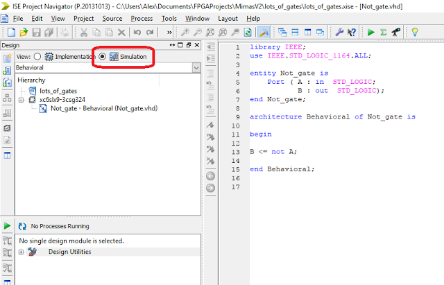
Click on the simulate radio button on the Hierarchy window:


Next right click on the Hierarchy window and select Add new source:


Select VHDL test bench and call the file something sensible...I called mine Not_gate_tb. Click Next when ready to continue:


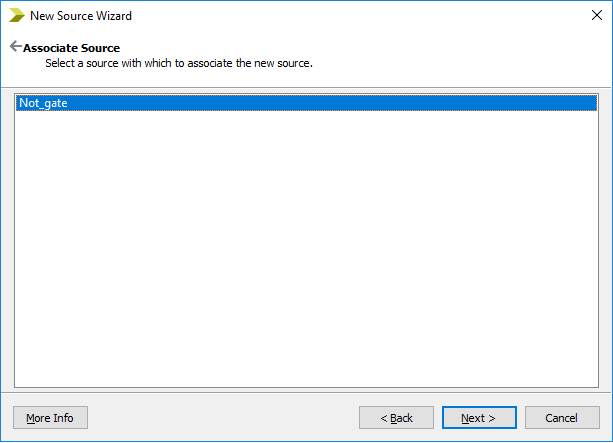
Associate the test bench source file with the code you wish to simulate...click Next when ready to continue:


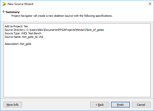
Click finish to continue and return to the main project window:


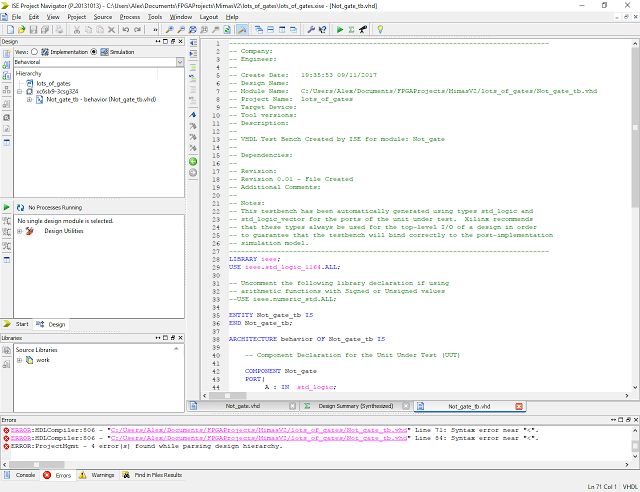
Helpfully Xilinx WebISE has automatically generated the test bench code for us...unhelpfully it has also introduced some errors. Don't worry about these for now...the code generated is expecting a clock source to be present. There isn't a clock source in our design as we did not need one. We will remove the errors when we modify the test bench code. Again I like remove the top comments as I don't need them. Comments are useful but only when necessary...

Here is the code with the comments removed:

LIBRARY ieee;
USE ieee.std_logic_1164.ALL;
 
ENTITY Not_gate_tb IS
END Not_gate_tb;
 
ARCHITECTURE behavior OF Not_gate_tb IS 
 
    -- Component Declaration for the Unit Under Test (UUT)
 
    COMPONENT Not_gate
    PORT(
         A : IN  std_logic;
         B : OUT  std_logic
        );
    END COMPONENT;
    

   --Inputs
   signal A : std_logic := '0';

  --Outputs
   signal B : std_logic;
   -- No clocks detected in port list. Replace <clock> below with 
   -- appropriate port name 
 
   constant <clock>_period : time := 10 ns;
 
BEGIN
 
 -- Instantiate the Unit Under Test (UUT)
   uut: Not_gate PORT MAP (
          A => A,
          B => B
        );

   -- Clock process definitions
   <clock>_process :process
   begin
  <clock> <= '0';
  wait for <clock>_period/2;
  <clock> <= '1';
  wait for <clock>_period/2;
   end process;
 

   -- Stimulus process
   stim_proc: process
   begin  
      -- hold reset state for 100 ns.
      wait for 100 ns; 

      wait for <clock>_period*10;

      -- insert stimulus here 

      wait;
   end process;
 
END;

Now we need to remove the code relating to the automatically generated clock as this isn't
required:

LIBRARY ieee;
USE ieee.std_logic_1164.ALL;
 
ENTITY Not_gate_tb IS
END Not_gate_tb;
 
ARCHITECTURE behavior OF Not_gate_tb IS 
 
    -- Component Declaration for the Unit Under Test (UUT)
 
    COMPONENT Not_gate
    PORT(
         A : IN  std_logic;
         B : OUT  std_logic
        );
    END COMPONENT;
    

   --Inputs
   signal A : std_logic := '0';

  --Outputs
   signal B : std_logic;
 
BEGIN
 
 -- Instantiate the Unit Under Test (UUT)
   uut: Not_gate PORT MAP (
          A => A,
          B => B
        );

   -- Stimulus process
   stim_proc: process
   begin  
      -- hold reset state for 100 ns.
      wait for 100 ns; 

      -- insert stimulus here 

      wait;
   end process;

END;

The code generated actually uses the component statement so our automatically generated code is a perfect example of how a statement should be used! In the architecture statement we can see the component declaration for the Not_gate. Below that section some internal signals are defined to connect to the component we would like to simulate. Underneath that section we have the instantiation section which creates a version of the not_gate called 'uut' and maps the internal signal connections to the component signal connections. Now we need to write some code in the stimulus process section which sets the A input signal to a known value so that the simulator can run the code in the Not_gate module and display what will happen at the output signal - B.

As the module is an inverter or not gate it should be obvious that whatever logic level is present at the output signal is the opposite or inverse of the input signal. For more complicated modules this might be more difficult to assess which is why simulation is useful. It is also possible to see if there are any timing or sequencing issues present with more complicated modules. Simulation can be a very useful diagnostic tool when developing FPGA code.

Let’s write the stimulus VHDL code to test the module code and provide the simulator some information. Let’s set the 'A' input of the inverter to logic '1' for 100 ns and then set it to logic '0' for 100 ns and then set it to an unknown logic level 'X' for 100 ns. When we run the simulator we will be able to visually see what the output signal 'B' does when presented with those input 'stimuli' or logic states.

*Stimuli - a latin word which is the plural of stimulus, to provide a specific functional reaction!

Here is the code:

-- Stimulus process
   stim_proc: process
   begin  
      -- hold reset state for 100 ns.
      wait for 100 ns; 

      A <= '1';
  wait for 100 ns; 
  
  A <= '0';
  wait for 100 ns;
  
  A <= 'X';
  wait for 100 ns;

      wait;
   end process;

Let’s save the code and run the simulator! Click on the Not_gate VHDL test bench module in the Hierarchy window:


Next right click on 'Behavioral Check Syntax' in the process window and select Run:


Once the process has completed there should be a green tick present:


Next right click on Simulate Behavioral Model and select Run:


Once the process has completed the ISIM screen will be displayed showing the results of the simulation:


At first it looks as though the simulation has failed as the result traces are red and in an X state - don't worry though that is what was expected. The last state we simulated was an 'X' state for the input signal. Click on the 'Zoom to Full View' icon on the toolbar to display the full results traces:


The green part of the traces show how the input 'A' went from a logic '0' to a logic '1' after 100 ns and the output 'B' changed accordingly. Then the input 'A' went from a logic '1' to a logic '0' for 100 ns and then the input 'A' was set to an unknown logic state 'X' and the output 'B' responded with a logic 'X' for the rest of the simulation - exactly what the test bench code was meant to do. So our simulation worked perfectly and more importantly the Not_gate module works perfectly!

This module can now be reused as many times as we like in any of our designs - Most Excellent!

Close down the ISIM application as we are finished with that program to return to the main project screen.

Let’s add some more logic functions like the AND, OR, and XOR functions. I'm not going to show all of the steps with pictures this time though, it's the same process as before.

Click on the implementation radio button and then add new VHDL source modules to the project. I called mine And_gate, Or_gate and XOR_gate. I chose to make them all two input devices with one output.


Here is the project window with all of the VHDL source file modules:


I deleted all of the comments that were not needed for each of the new modules and added the necessary code for the architecture sections. The code should be pretty self-explanatory but just in case here is the VHDL code for each logic function:

And Gate logic function VHDL code:

library IEEE;
use IEEE.STD_LOGIC_1164.ALL;

entity And_Gate is
    Port ( A : in  STD_LOGIC;
           B : in  STD_LOGIC;
           Q : out  STD_LOGIC);
end And_Gate;

architecture Behavioral of And_Gate is

begin

   Q <= A and B;

end Behavioral;

Or Gate logic function VHDL code:

library IEEE;
use IEEE.STD_LOGIC_1164.ALL;

entity Or_gate is
    Port ( A : in  STD_LOGIC;
           B : in  STD_LOGIC;
           Q : out  STD_LOGIC);
end Or_gate;

architecture Behavioral of Or_gate is

begin

Q <= A or B;

end Behavioral;

Xor Gate logic function VHDL code:

library IEEE;
use IEEE.STD_LOGIC_1164.ALL;

entity Xor_gate is
    Port ( A : in  STD_LOGIC;
           B : in  STD_LOGIC;
           Q : out  STD_LOGIC);
end Xor_gate;

architecture Behavioral of Xor_gate is

begin

Q <= A xor B;

end Behavioral;

Ensure each VHDL module has the correct code. If you were so inclined you could then simulate each module to make certain the code behaves as intended. I'm not going to bother this time but for more complicated modules it's very important that it's simulated. I have saved myself hours of debugging by simulating the module behaviour before continuing.

At this point I like to draw a diagram which shows what function I want all of these modules to perform when connected together. Normally I would do this before I start writing the code but as this is just an example I'm doing it now. Lets implement each logic gate into the FPGA and use the DIP switches to connect to the inputs of the logic gates and then lets connect the outputs of the logic gates to the LEDS so that we can see the results when we change the state of the DIP switches!


From the diagram we can now create a VHDL top module which will connect to the DIP switches and LED and we can then make components to call all of the other modules and connect those modules inputs and outputs to the top module's inputs and outputs. Sounds complicated but it is actually fairly simple. Lets create the top module by right clicking in the hierarchy window as before...I called mine lots_of_gates_top_module:


Click Next and lets select how many inputs and outputs we will need. We need one input and output for the Not gate, two inputs and one output for the And gate, Or gate and Xor gate. So that makes seven inputs and four outputs. Give the inputs and outputs sensible names:


Click next to display the summary screen:


Click Finish to return to the main project screen.


Again remove the comments that are not necessary. Add comments later if required...


Now we need to add the component statements in the architecture section. The first
component we want to add is the Not gate. There is a really cool and easy way to do this thanks to Xilinx WebISE all we have to do is click on the module we want to use and then click on the Design Utilities option in the process window and double click on 'View HDL Instantiation Template':


We can then select and copy the code without the comments and paste it into the architecture section of the top module. It saves typing and it's completely correct! All we then need to do is correctly complete the port map section and our first component is done:


The Not_gate component signal connections map to the Not_input signal and the Not_Output_LED signal. I also changed the component instantiation label to something more meaningful. It can get awkward when you have multiple components of the same type if you don't use a sensible naming convention:


Repeat the process for all of the other components we intend to add. Once you have done that we need to move the instantiation sections to the begin and end section of the architecture statement. Once complete the code should look like this:


library IEEE;
use IEEE.STD_LOGIC_1164.ALL;

entity lots_of_gates_top_module is
    Port ( Not_input : in  STD_LOGIC;
           Not_Output_LED : out  STD_LOGIC;
          
     And_A_Input : in  STD_LOGIC;
           And_B_Input : in  STD_LOGIC;
           And_Q_Output_LED : out  STD_LOGIC;
          
     Or_A_Input : in  STD_LOGIC;
           Or_B_Input : in  STD_LOGIC;
           Or_Q_Output_LED : out  STD_LOGIC;
          
     Xor_A_Input : in  STD_LOGIC;
           Xor_B_Input : in  STD_LOGIC;
           Xor_Q_Output_LED : out  STD_LOGIC);
end lots_of_gates_top_module;

architecture Behavioral of lots_of_gates_top_module is

 COMPONENT Not_gate
 PORT(
  A : IN std_logic;         
  B : OUT std_logic
  );
 END COMPONENT;

 COMPONENT And_Gate
 PORT(
  A : IN std_logic;
  B : IN std_logic;         
  Q : OUT std_logic
  );
 END COMPONENT;

 COMPONENT Or_gate
 PORT(
  A : IN std_logic;
  B : IN std_logic;         
  Q : OUT std_logic
  );
 END COMPONENT;

 COMPONENT Xor_gate
 PORT(
  A : IN std_logic;
  B : IN std_logic;         
  Q : OUT std_logic
  );
 END COMPONENT;

begin

 Not_gate_1: Not_gate PORT MAP(
  A => Not_input,
  B => Not_Output_LED
 );

 And_Gate_1: And_Gate PORT MAP(
  A => And_A_Input,
  B => And_B_Input,
  Q => And_Q_Output_LED
 );

 Or_gate_1: Or_gate PORT MAP(
  A => Or_A_Input,
  B => Or_B_Input,
  Q => Or_Q_Output_LED
 );

 Xor_gate_1: Xor_gate PORT MAP(
  A => Xor_A_Input,
  B => Xor_B_Input,
  Q => Xor_Q_Output_LED
 );

end Behavioral; 

The code should be fairly self-explanatory. Save the module and now let’s simulate it to make sure it will work as intended. Using the same process as before let’s create a test bench forthe top module and make sure that everything will work.

Click on the simulate radio button in the hierarchy window and then add a new source, select VHDL test bench and give it a suitable name. I called mine lots_gates_test_bench. Then associate the module with the lots_of_gates VHDL module and click finish. Then WebISE will generate some code for us. Delete the comments as necessary. After that delete the clock sections as we don't need those sections.

Finally all that is needed is to write the stimuli section like before. Lets exercise each gate in turn with suitable logic levels and allow time for each state to be easily viewed on the simulator screen. We could exercise all the gates at once but I prefer to see each state separately.

Here is the stimulus code:

library IEEE;
use IEEE.STD_LOGIC_1164.ALL;

entity lots_of_gates_top_module is
    Port ( Not_input : in  STD_LOGIC;
           Not_Output_LED : out  STD_LOGIC;
          
     And_A_Input : in  STD_LOGIC;
           And_B_Input : in  STD_LOGIC;
           And_Q_Output_LED : out  STD_LOGIC;
          
     Or_A_Input : in  STD_LOGIC;
           Or_B_Input : in  STD_LOGIC;
           Or_Q_Output_LED : out  STD_LOGIC;
          
     Xor_A_Input : in  STD_LOGIC;
           Xor_B_Input : in  STD_LOGIC;
           Xor_Q_Output_LED : out  STD_LOGIC);
end lots_of_gates_top_module;

architecture Behavioral of lots_of_gates_top_module is

 COMPONENT Not_gate
 PORT(
  A : IN std_logic;         
  B : OUT std_logic
  );
 END COMPONENT;

 COMPONENT And_Gate
 PORT(
  A : IN std_logic;
  B : IN std_logic;         
  Q : OUT std_logic
  );
 END COMPONENT;

 COMPONENT Or_gate
 PORT(
  A : IN std_logic;
  B : IN std_logic;         
  Q : OUT std_logic
  );
 END COMPONENT;

 COMPONENT Xor_gate
 PORT(
  A : IN std_logic;
  B : IN std_logic;         
  Q : OUT std_logic
  );
 END COMPONENT;

begin

 Not_gate_1: Not_gate PORT MAP(
  A => Not_input,
  B => Not_Output_LED
 );

 And_Gate_1: And_Gate PORT MAP(
  A => And_A_Input,
  B => And_B_Input,
  Q => And_Q_Output_LED
 );

 Or_gate_1: Or_gate PORT MAP(
  A => Or_A_Input,
  B => Or_B_Input,
  Q => Or_Q_Output_LED
 );

 Xor_gate_1: Xor_gate PORT MAP(
  A => Xor_A_Input,
  B => Xor_B_Input,
  Q => Xor_Q_Output_LED
 );

end Behavioral; 

Let’s check the syntax and run the simulator!

Here is the result, I did manipulate the traces to put the outputs next to the inputs:


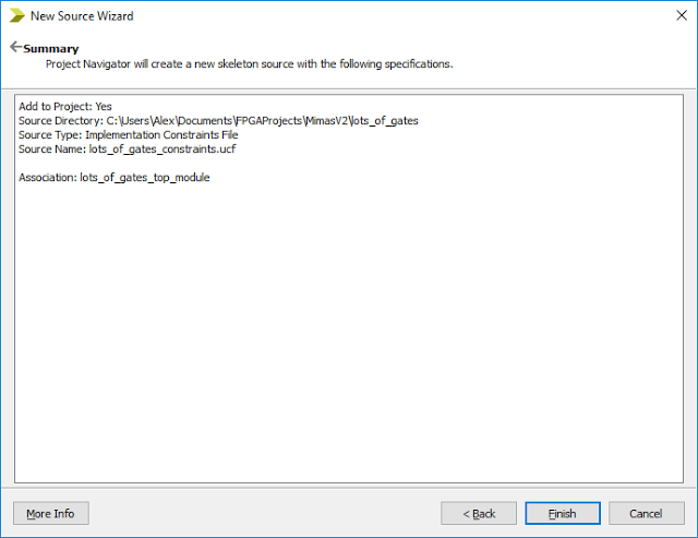
Close down the simulator...It’s time for the final bit of code writing - creating the implementation constraints file to tell WebISE how the external devices will connect to the FPGA signals in our design. In the hierarchy window click on add new source and choose implementation constraints file:


Click next to continue:


Click Finish to return to the main project screen. Now we need to decide how we want our DIP switches and LEDS to connect to our inputs and outputs.
  • Let’s set DIP switch 0 to be the Not gate input
  • Let’s set LED 0 to be the Not gate output
  • Let’s set DIP switch 1 to be the AND gate A input
  • Let’s set DIP switch 2 to be the AND gate B input
  • Let’s set LED 1 to be the AND gate Output
  • Let’s set DIP switch 3 to be the OR gate A input
  • Let’s set DIP switch 4 to be the OR gate B input
  • Let’s set LED 3 to be the OR gate Output
  • Let’s set DIP switch 5 to be the XOR gate A input
  • Let’s set DIP switch 6 to be the XOR gate B input
  • Let’s set LED 5 to be the XOR gate Output
It is possible to use the WebISE software to generate the constraints for us but I prefer to write my own code using the supplied constraints file from Numato Labs as a template.

Here is the code:

#++++++++++++++++++++++++++++++++++++++++++++++++++++++++++++++++++#
# This file is a .ucf for Mimas V2                                 #
# To use it in your project :                                      #
# * Remove or comment the lines corresponding to unused pins in    #
# the 
project                                                      #

# * Rename the used signals according to the your project          #
#++++++++++++++++++++++++++++++++++++++++++++++++++++++++++++++++++#

CONFIG VCCAUX = "3.3" ;
#NET "CLK" LOC = V10 | IOSTANDARD = LVCMOS33 | PERIOD = 100MHz;
#NET "RST_n" IOSTANDARD = LVCMOS33 | PULLUP;

#################################################################################
# DIP Switches                                                                  #
#################################################################################

NET "Not_input" LOC = C17 | IOSTANDARD = LVCMOS33 | DRIVE = 8 | SLEW = FAST | PULLUP;
NET "And_A_Input" LOC = C18 | IOSTANDARD = LVCMOS33 | DRIVE = 8SLEW = FAST | PULLUP;
NET "And_B_Input" LOC = D17 | IOSTANDARD = LVCMOS33 | DRIVE = 8SLEW = FAST | PULLUP;
NET "Or_A_Input" LOC = D18 | IOSTANDARD = LVCMOS33 | DRIVE = 8SLEW = FAST | PULLUP;
NET "Or_B_Input" LOC = E18 | IOSTANDARD = LVCMOS33 | DRIVE = 8SLEW = FAST | PULLUP;
NET "Xor_A_Input" LOC = E16 | IOSTANDARD = LVCMOS33 | DRIVE = 8SLEW = FAST | PULLUP;
NET "Xor_B_Input" LOC = F18 | IOSTANDARD = LVCMOS33 | DRIVE = 8SLEW = FAST | PULLUP;

#################################################################################
# LEDs                                                                          #
#################################################################################

NET "Not_Output_LED" LOC = P15 | IOSTANDARD = LVCMOS33 | DRIVE = 8SLEW = FAST;
NET "And_Q_Output_LED" LOC = N15 | IOSTANDARD = LVCMOS33 | DRIVE = 8SLEW = FAST;
NET "Or_Q_Output_LED" LOC = U17 | IOSTANDARD = LVCMOS33 | DRIVE = 8SLEW = FAST;
NET "Xor_Q_Output_LED" LOC = T17 | IOSTANDARD = LVCMOS33 | DRIVE = 8SLEW = FAST;

Copy and paste the above code into the constraints file and then Save the file! It's now time to check everything is correct and implement everything before creating a bit stream file and upload it to the Mimas V2....

Click on the green arrow in the process window to process all of the code. Once complete there should be green tick marks on each section:


Next right click on Generate Programming File and Process Properties and select create Binary Configuration file:


Click Ok and then Right click on Generate Programming file and select run:


Once that has completed - connect up the Mimas V2 development board to your computer and load up the Mimas V2 Config tool. Select the correct COM port and finally navigate to the recently created Bit Stream file called 'lots_of_gates_top_module.bin' and click Upload:


It may take a while...I hear that programming the Mimas V2 using a JTAG programmer is considerably faster! Once that has completed lets test it out!

Remember that the Mimas V2 Logic levels are active low. So the LEDS will be off when a logic '1' is present at the output.
  • If you manipulate DIP switch 8 - the D1 LED will change state
  • If you manipulate DIP switches 6 and 7 - the D3 LED will change state (AND function)
  • If you manipulate DIP switches 4 and 5 - the D5 LED will change state (OR function)
  • If you manipulate DIP switches 2 and 3 - the D7 LED will change state (XOR function)
The project uploaded to the Mimas V2 and working!
Well that's about it for now...Apologies for the really long post. I couldn't really find a way to make it much shorter. If you want to be adventurous change the code to have multiple NOT gates, or AND gates etc....it only requires changing the instantiation sections with a single component declaration, you will need to map the pins though.

If people need access to the project and files it's here:
https://drive.google.com/open?id=0B7fA8ZgAyKMlaHo5Qms2YjhtNW8

That's all for now people - take care, Langster!