Mimas V2 FPGA - Controlling a 16x2 LCD Display
This post discusses the same subject but goes into more detail and relies on VHDL code instead of Verilog.
There are a great many 16x2 LCD displays available to electronic design engineers. Nearly all of them are controlled by the Hitachi HD44780 control IC which is built into the display module. The wikipedia entry on the control system is here:
Wikipedia Entry on HD44780
The datasheet for the HD44780 is here:
HD44780 datasheet
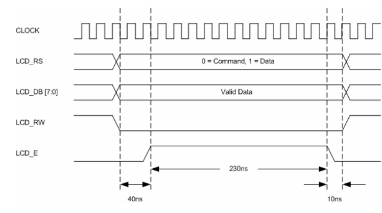
The pins used on LCD display have been standardised to make it simple for engineers to use these displays in their electronic circuits. The nuances of controlling a display are quite complex and beyond the scope of what I'm prepared to discuss here. The displays are controlled by sending signals from a microcontroller which implements a state machine in order to send data to be displayed to the display and read back from the display.
If people are interested in exactly how to control an LCD display with switches then here is a tutorial for you:
HD44780 Tutorial
In order to use an FPGA to achieve control of a display we need to implement a similar state machine. This has been written many times before and a particular good paper explaining the implementation of the state machine is here:
FPGA State machine paper
Luckily we don't have to write our own state machine as I found a really good implementation of one at OpenCores. OpenCores is an excellent FPGA design and development resource and if anyone is serious about learning and using FPGA technology then they should check it out!
http://opencores.org/
In order to use the site you will have to register but that's no hardship as registration is simple and free!
The project we are interested in is here:
http://opencores.org/project,16x2_lcd_controller
Download the project files and extract them to somewhere sensible on your Hard disk and then load up Xilinx WebISE and lets get started!
We need to create a new project - use the settings shown in the picture below:

They are all correct for the Numato Labs Mimas V2 Development board. Click OK when ready.
Next right click on the Hierarchy window in the main project window of WebISE and choose 'add Copy of Source' - then navigate to the folder(s) where the OpenCores project is located and find and then add the file:
lcd16x2_ctrl.vhd

Click 'OK' when asked to confirm adding the file to the project.
Then repeat the process to add lcd16x2_ctrl_demo.vhd

Click 'OK' when asked to confirm adding the file to the project.
The repeat the process on more time to add the UCF file called 'pin_locations.ucf'

The main project window should now look like this:

What needs to be done now is to update the UCF file with the appropriate connections for the Mimas V2 Development board. Load up the UCF file in the internal text editor in WebISE:

Delete all of the text present and replace it with the code below:
#+++++++++++++++++++++++++++++++++++++++++++++++++++++++++++++++++++++++++++++++++++++++++++#
# This file is a .ucf for 16x2 LCD Expansion Modules on Mimas V2 modified by ALEX! #
# To use it in your project : #
# * Remove or comment the lines corresponding to unused pins #
# * Rename the used signals according to the your project #
#+++++++++++++++++++++++++++++++++++++++++++++++++++++++++++++++++++++++++++++++++++++++++++#
# Clock 100 MHz
NET "Clk" LOC = V10 | IOSTANDARD = LVCMOS33 | Period = 100 MHz;
###########################################################################################################
# 16x2 LCD Expansion Module #
###########################################################################################################
###########################################################################################################
# Expansion Connector's HEADER P6 #
###########################################################################################################
# Clock 100 MHz
NET "clk" LOC = V10 | IOSTANDARD = LVCMOS33 | Period = 100 MHz;
NET "lcd_e" LOC = T4 | IOSTANDARD = LVCMOS33 | DRIVE = 8 | SLEW = FAST; # Enable PIN of LCD
NET "lcd_rs" LOC = V7 | IOSTANDARD = LVCMOS33 | DRIVE = 8 | SLEW = FAST; # Register Select PIN of LCD
NET "lcd_rw" LOC = U7 | IOSTANDARD = LVCMOS33 | DRIVE = 8 | SLEW = FAST; # Read/Write PIN of LCD
# Four bits LCD Data
NET "lcd_db<7>" LOC = R3 | IOSTANDARD = LVCMOS33 | DRIVE = 8 | SLEW = FAST; # PIN 14 on LCD
NET "lcd_db<6>" LOC = V5 | IOSTANDARD = LVCMOS33 | DRIVE = 8 | SLEW = FAST; # PIN 13 on LCD
NET "lcd_db<5>" LOC = U5 | IOSTANDARD = LVCMOS33 | DRIVE = 8 | SLEW = FAST; # PIN 12 on LCD
NET "lcd_db<4>" LOC = V4 | IOSTANDARD = LVCMOS33 | DRIVE = 8 | SLEW = FAST; # PIN 11 on LCD
Then save the project - always a good idea. Now its time to 'compile' the code! Implement a top module by clicking on the green arrrow:

Now generate a bitstream file:

Once that is complete generate a 'Bit File' and then upload that to the Mimas V2 Development board via your preferred method - by Python Script or by using the supplied uploader. I use the uploader.

Ensure you have a power supply connected to the Vext input of the Expansion PCB (which is capable of supplying at least 7 Volts. Then plug the expansion header into the P6 header socket. When you connect it up you should be presented with the following image:

Cool beans!
At this point I should probably explain some of the code and how it works. We added three files to the project in order to get things working.
- lcd16x2_ctrl.vhd - The state machine for controlling the LCD display
- pin_locations.UCF - The UCF file which tells the compiler
- lcd16x2_ctrl_demo.vhd - a file to demonstrate the display in operation.
The code was written by a very clever German gentleman named Daniel Drescher and full credit goes to him for an excellent implementation of an VHDL Hitachi HD44780 display driver.
I'm not going to go into much detail about the lcd16x2_ctrl.vhd file except to say that it provides the method for controlling the pins on the display to go about getting the response required whether reading whether the display has correctly displayed something or writing data to the display. Most people are only interested in write operation however the read operation can be useful for fault finding.
The file pin_locations.ucf tell Xilinx WebISE which pins on the FPGA are going to be used. In the example above we used the pins associated with the P6 connector. If another connector is needed then refer to the Mimas V2 instruction manual and schematic and update this file as necessary.
The 16x2_ctrl_demo.vhd file is the file of most interest. It allows the designer to set the data to be sent and displayed on the 16x2 screen.
library ieee;
use ieee.std_logic_1164.all;
-------------------------------------------------------------------------------
entity lcd16x2_ctrl_demo is
port (
clk : in std_logic;
lcd_e : out std_logic;
lcd_rs : out std_logic;
lcd_rw : out std_logic;
lcd_db : out std_logic_vector(7 downto 4));
end entity lcd16x2_ctrl_demo;
-------------------------------------------------------------------------------
The above lines of code tell the compiler to include some standard vhdl libraries and then implements an entity statement - tells the compiler the pin names we are going to use and what type of pin they are either input or output. The pin names point towards their function.
clk - The free running clock to assist with the timings to control the display
lcd_e - the LCD enable pin
lcd_rs - the LCD register select pin
lcd_rw - the LCD read/write register pin
lcd_db - 4 pins used to control the data pins on the LCD display in 4 bit operation
-------------------------------------------------------------------------------
architecture behavior of lcd16x2_ctrl_demo is
--
signal timer : natural range 0 to 100000000 := 0;
signal switch_lines : std_logic := '0';
signal line1 : std_logic_vector(127 downto 0);
signal line2 : std_logic_vector(127 downto 0);
-- component generics
constant CLK_PERIOD_NS : positive := 10; -- 100 Mhz
-- component ports
signal rst : std_logic;
signal line1_buffer : std_logic_vector(127 downto 0);
signal line2_buffer : std_logic_vector(127 downto 0);
The above lines are from the architecture statement. It defines the behaviour of the FPGA. In this case it will drive the 16x2 LCD display. It does this by implementing some internal signals (variables).
The Signal timer is a timer which counts from zero to ten million. This will be used to ensure that the timings for the reading and writing to the display are correct,
The signal switch lines is a variable to tell the FPGA to swap the top and bottom lines on the 16x2 LCD display.
The signals line1 and line2 are logic vectors to send the characters to be displayed to the 16x2 LCD display.
Next a constant clock period is set at 100 MHz or ten nano seconds and the clock is positive edge triggered.
Finally some further signals are created including a reset signal and some logic buffers for the characters to be sent to the 16x2 Display.
-------------------------------------------------------------------------------
begin -- architecture behavior
-- component instantiation
DUT : entity work.lcd16x2_ctrl
generic map (
CLK_PERIOD_NS => CLK_PERIOD_NS)
port map (
clk => clk,
rst => rst,
lcd_e => lcd_e,
lcd_rs => lcd_rs,
lcd_rw => lcd_rw,
lcd_db => lcd_db,
line1_buffer => line1_buffer,
line2_buffer => line2_buffer);
rst <= '0';
The above lines begin the actual architecture statement. The method of controlling the display is instantiated from the code written in lcd16x2_ctrl.vhd. The clock period is set to match and the pins are mapped to ensure data is passed correctly between the two files. Finally the reset pin is set low to ensure the display is ready to receive data.
-------------------------------------------------------------------------------
-- see the display's datasheet for the character map
line1(127 downto 120) <= X"20";
line1(119 downto 112) <= X"20";
line1(111 downto 104) <= X"48"; -- H
line1(103 downto 96) <= X"65"; -- e
line1(95 downto 88) <= X"6c"; -- l
line1(87 downto 80) <= X"6c"; -- l
line1(79 downto 72) <= X"6f"; -- o
line1(71 downto 64) <= X"20";
line1(63 downto 56) <= X"57"; -- W
line1(55 downto 48) <= X"6f"; -- o
line1(47 downto 40) <= X"72"; -- r
line1(39 downto 32) <= X"6c"; -- l
line1(31 downto 24) <= X"64"; -- d
line1(23 downto 16) <= X"21"; -- !
line1(15 downto 8) <= X"20";
line1(7 downto 0) <= X"20";
line2(127 downto 120) <= X"30";
line2(119 downto 112) <= X"31";
line2(111 downto 104) <= X"32";
line2(103 downto 96) <= X"33";
line2(95 downto 88) <= X"34";
line2(87 downto 80) <= X"35";
line2(79 downto 72) <= X"36";
line2(71 downto 64) <= X"37";
line2(63 downto 56) <= X"38";
line2(55 downto 48) <= X"39";
line2(47 downto 40) <= X"3a";
line2(39 downto 32) <= X"3b";
line2(31 downto 24) <= X"3c";
line2(23 downto 16) <= X"3d";
line2(15 downto 8) <= X"3e";
line2(7 downto 0) <= X"3f";
line1_buffer <= line2 when switch_lines = '1' else line1;
line2_buffer <= line1 when switch_lines = '1' else line2;
The above lines actually are the characters that will be sent to the display. The more observant will notice that the values used are hexadecimal values for ascii characters. If it was required to change the characters displayed on screen we would need to change these hexadecimal values to whatever we wanted.
-------------------------------------------------------------------------------
-- switch lines every second
process(clk)
begin
if rising_edge(clk) then
if timer = 0 then
timer <= 100000000;
switch_lines <= not switch_lines;
else
timer <= timer - 1;
end if;
end if;
end process;
end architecture behavior;
The above lines is the actual process the display will follow. If the clock is positive and the timer is at zero then the timer is set to a hundred million. This equates to one second as 100,000,000 counts of a 100 MHz clock is one second. The characters on the top and bottom lines are swapped. Then the timer is decremented and the process ends.
If we wanted to change the characters being displayed we need to change the section shown here:
-- see the display's datasheet for the character map
line1(127 downto 120) <= X"20";
line1(119 downto 112) <= X"20";
line1(111 downto 104) <= X"48"; -- H
line1(103 downto 96) <= X"65"; -- e
line1(95 downto 88) <= X"6c"; -- l
line1(87 downto 80) <= X"6c"; -- l
line1(79 downto 72) <= X"6f"; -- o
line1(71 downto 64) <= X"20";
line1(63 downto 56) <= X"57"; -- W
line1(55 downto 48) <= X"6f"; -- o
line1(47 downto 40) <= X"72"; -- r
line1(39 downto 32) <= X"6c"; -- l
line1(31 downto 24) <= X"64"; -- d
line1(23 downto 16) <= X"21"; -- !
line1(15 downto 8) <= X"20";
line1(7 downto 0) <= X"20";
line2(127 downto 120) <= X"30";
line2(119 downto 112) <= X"31";
line2(111 downto 104) <= X"32";
line2(103 downto 96) <= X"33";
line2(95 downto 88) <= X"34";
line2(87 downto 80) <= X"35";
line2(79 downto 72) <= X"36";
line2(71 downto 64) <= X"37";
line2(63 downto 56) <= X"38";
line2(55 downto 48) <= X"39";
line2(47 downto 40) <= X"3a";
line2(39 downto 32) <= X"3b";
line2(31 downto 24) <= X"3c";
line2(23 downto 16) <= X"3d";
line2(15 downto 8) <= X"3e";
line2(7 downto 0) <= X"3f";
It really helps to have an ascii character map with the hexadecimal values:
Just for fun, I changed the code to this:
-- see the display's datasheet for the character map
line1(127 downto 120) <= X"4E"; -- N
line1(119 downto 112) <= X"75"; -- u
line1(111 downto 104) <= X"6D"; -- m
line1(103 downto 96) <= X"61"; -- a
line1(95 downto 88) <= X"74"; -- t
line1(87 downto 80) <= X"6F"; -- o
line1(79 downto 72) <= X"20"; -- space
line1(71 downto 64) <= X"4C"; -- L
line1(63 downto 56) <= X"61"; -- a
line1(55 downto 48) <= X"62"; -- b
line1(47 downto 40) <= X"73"; -- s
line1(39 downto 32) <= X"20"; -- space
line1(31 downto 24) <= X"46"; -- F
line1(23 downto 16) <= X"50"; -- P
line1(15 downto 8) <= X"47"; -- G
line1(7 downto 0) <= X"41"; -- A
line2(127 downto 120) <= X"56"; -- V
line2(119 downto 112) <= X"48"; -- H
line2(111 downto 104) <= X"44"; -- D
line2(103 downto 96) <= X"4C"; -- L
line2(95 downto 88) <= X"20"; -- space
line2(87 downto 80) <= X"4C"; -- L
line2(79 downto 72) <= X"43"; -- C
line2(71 downto 64) <= X"44"; -- D
line2(63 downto 56) <= X"20"; -- space
line2(55 downto 48) <= X"45"; -- E
line2(47 downto 40) <= X"78"; -- x
line2(39 downto 32) <= X"61"; -- a
line2(31 downto 24) <= X"6D"; -- m
line2(23 downto 16) <= X"70"; -- p
line2(15 downto 8) <= X"6C"; -- l
line2(7 downto 0) <= X"65"; -- e
I then recompiled and uploaded the new bitstream file to the FPGA development board. Here is a quick video showing what happened:
Well that's all for now. Hope this helps people out! Here is the code if people need it:
Cheers - Langster!
can i apply the same steps to cyclone2 ep2c5 (miniboard)
ReplyDeleteIn theory you could. The VHDL code is transferrable to other FPGA devices. You will need to generate the implementation constraints file for the cyclone2 Ep3c5 board - I have no experience of this device so cannot provide much assistance. Next you will need to modify the VHDL code to cover the connections you are going to make - Good luck!
Delete