There comes a point in FPGA programming where trying to put all of the code in one single source file becomes really awkward. The file would become very long to read and debug and it may make more sense to take a modular approach and re-use code from previous designs. Luckily for the FPGA design engineer it is possible to write and design modules in VHDL very easily and each module can be tested and used on it's own.
The way to implement this is to use the component keyword in VHDL and 'instantiate' as many of the modules or blocks of code as one wants.
In previous posts I have already used this method but I haven't really ever discussed it explicitly so here goes:
In a VHDL source module the code is organised into section statements known as:
- Entities - The statement which defines the external input and output connections of the module.
- Architectures - This is the code section which actually tells or defines the function of the module.
- Components - A statement within the architecture section which allows the designer to link internal signals or external signals with pre-written VHDL code in another module.
- Instances - A statement which actually creates the 'instance' of the external module code within another module. A designer can have multiple instances of a module within a design with one component statement as long as all of the connections are correctly port mapped.
entity EntitySection is
Port ( clkinput : in STD_LOGIC;
input1 : in STD_LOGIC;
input2 : in STD_LOGIC;
input3 : in STD_LOGIC;
output1 : out STD_LOGIC;
output2 : out STD_LOGIC);
end EntitySection;Here is an example of an Architecture statement:
architecture Behavioral of EntitySection is
begin
input1 <= not input2;
end Behavioral;
This is the section of code that defines how the internal signals and external signals will interact to realise the function required. As before the green text are keywords, the red text are labels and the black text are the inputs and outputs.
Here is an example of a Component statement:
COMPONENT Not_gate
PORT( input1 : IN std_logic;
output1 : OUT std_logic);
END COMPONENT;
As above, the different colours relate to keywords, labels, definitions and types.
Here is an example of a Instantiation statement:
Inst_Not_gate: Not_gate
PORT MAP(
input1 => input_signal1,
output1 => output_signal1
);
The instantiation code is the way the designer defines how the signals from the component module connect to the signals within the source module. These signals in the source module could be internal or external signals.
As an example lets write some simple two input logic gates in VHDL code and then'instantiate multiple versions of them in VHDL and then simulate their function and then finally show the results working on the Mimas V2 FPGA Development board. In theory any FPGA development board could be made to work including the Elbert V2 (I will share the Elbert V2 version also as I know some people are using those boards).
Load up Xilinx WebISE and start a new project - I called mine Lots of gates and placed it in a suitable folder on the hard disk.

Click next when ready to continue...

Input the settings shown (These are correct for the Numato Labs Mimas V2 development board).
Then click next when ready...

Click Finish to return to the main project screen within Xilinx WebISE:

Next right click on the Hierarchy window and select Add new source:

Select VHDL source module and give it a suitable name - I called mine Not_gate:

Click Next when ready to continue and enter the inputs and outputs for the Not_gate module. I chose to have an input and an output - to create a single inverter.

Click Next when ready to continue and display the summary page:

Click Finish to return to the main project window:

The WebISE software has helpfully created some code for us based on the decisions we made. I like to delete the comments (green text) as I don't find them helpful:

Now we need to write the architecture statement to make the module behave as an inverter or Not gate. It is very simple as the inverter function is already present within VHDL. Here is the code for the entire module:
library IEEE;
use IEEE.STD_LOGIC_1164.ALL;
entity Not_gate is
Port ( A : in STD_LOGIC;
B : out STD_LOGIC);
end Not_gate;
architecture Behavioral of Not_gate is
begin
B <= not A;
end Behavioral;
Now save the module - just in case...and then right click on the synthesize – XST process and select run. The software checks the code written is correct. Once the process has completed there will be a green tick on that section:

Now let’s simulate the code we have just written to ensure it works properly before we use it. It's always a good idea to simulate things to make sure that it works as intended.
Click on the simulate radio button on the Hierarchy window:

Next right click on the Hierarchy window and select Add new source:


Select VHDL test bench and call the file something sensible...I called mine Not_gate_tb. Click Next when ready to continue:
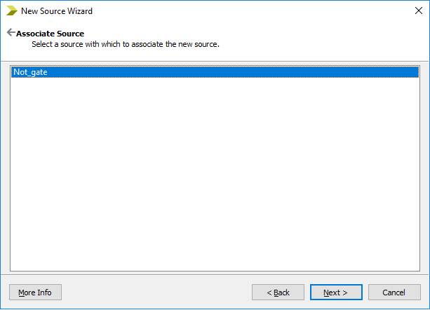
Associate the test bench source file with the code you wish to simulate...click Next when ready to continue:
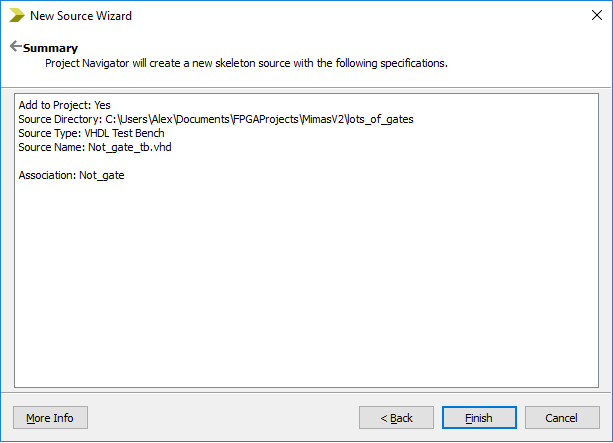
Click finish to continue and return to the main project window:
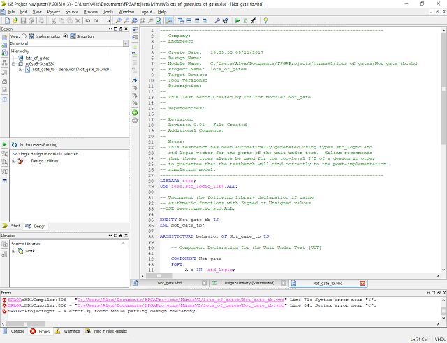
Helpfully Xilinx WebISE has automatically generated the test bench code for us...unhelpfully it has also introduced some errors. Don't worry about these for now...the code generated is expecting a clock source to be present. There isn't a clock source in our design as we did not need one. We will remove the errors when we modify the test bench code. Again I like remove the top comments as I don't need them. Comments are useful but only when necessary...
Here is the code with the comments removed:
Now we need to remove the code relating to the automatically generated clock as this isn't
required:
The code generated actually uses the component statement so our automatically generated code is a perfect example of how a statement should be used! In the architecture statement we can see the component declaration for the Not_gate. Below that section some internal signals are defined to connect to the component we would like to simulate. Underneath that section we have the instantiation section which creates a version of the not_gate called 'uut' and maps the internal signal connections to the component signal connections. Now we need to write some code in the stimulus process section which sets the A input signal to a known value so that the simulator can run the code in the Not_gate module and display what will happen at the output signal - B.
As the module is an inverter or not gate it should be obvious that whatever logic level is present at the output signal is the opposite or inverse of the input signal. For more complicated modules this might be more difficult to assess which is why simulation is useful. It is also possible to see if there are any timing or sequencing issues present with more complicated modules. Simulation can be a very useful diagnostic tool when developing FPGA code.
Let’s write the stimulus VHDL code to test the module code and provide the simulator some information. Let’s set the 'A' input of the inverter to logic '1' for 100 ns and then set it to logic '0' for 100 ns and then set it to an unknown logic level 'X' for 100 ns. When we run the simulator we will be able to visually see what the output signal 'B' does when presented with those input 'stimuli' or logic states.
*Stimuli - a latin word which is the plural of stimulus, to provide a specific functional reaction!
Here is the code:
Let’s save the code and run the simulator! Click on the Not_gate VHDL test bench module in the Hierarchy window:

Next right click on 'Behavioral Check Syntax' in the process window and select Run:

Once the process has completed there should be a green tick present:

Next right click on Simulate Behavioral Model and select Run:

Once the process has completed the ISIM screen will be displayed showing the results of the simulation:

At first it looks as though the simulation has failed as the result traces are red and in an X state - don't worry though that is what was expected. The last state we simulated was an 'X' state for the input signal. Click on the 'Zoom to Full View' icon on the toolbar to display the full results traces:

The green part of the traces show how the input 'A' went from a logic '0' to a logic '1' after 100 ns and the output 'B' changed accordingly. Then the input 'A' went from a logic '1' to a logic '0' for 100 ns and then the input 'A' was set to an unknown logic state 'X' and the output 'B' responded with a logic 'X' for the rest of the simulation - exactly what the test bench code was meant to do. So our simulation worked perfectly and more importantly the Not_gate module works perfectly!
This module can now be reused as many times as we like in any of our designs - Most Excellent!
Close down the ISIM application as we are finished with that program to return to the main project screen.
Let’s add some more logic functions like the AND, OR, and XOR functions. I'm not going to show all of the steps with pictures this time though, it's the same process as before.
Click on the implementation radio button and then add new VHDL source modules to the project. I called mine And_gate, Or_gate and XOR_gate. I chose to make them all two input devices with one output.

Here is the project window with all of the VHDL source file modules:

I deleted all of the comments that were not needed for each of the new modules and added the necessary code for the architecture sections. The code should be pretty self-explanatory but just in case here is the VHDL code for each logic function:
And Gate logic function VHDL code:
end Behavioral;
Or Gate logic function VHDL code:
end Behavioral;
Xor Gate logic function VHDL code:
end Behavioral;
Ensure each VHDL module has the correct code. If you were so inclined you could then simulate each module to make certain the code behaves as intended. I'm not going to bother this time but for more complicated modules it's very important that it's simulated. I have saved myself hours of debugging by simulating the module behaviour before continuing.
At this point I like to draw a diagram which shows what function I want all of these modules to perform when connected together. Normally I would do this before I start writing the code but as this is just an example I'm doing it now. Lets implement each logic gate into the FPGA and use the DIP switches to connect to the inputs of the logic gates and then lets connect the outputs of the logic gates to the LEDS so that we can see the results when we change the state of the DIP switches!

From the diagram we can now create a VHDL top module which will connect to the DIP switches and LED and we can then make components to call all of the other modules and connect those modules inputs and outputs to the top module's inputs and outputs. Sounds complicated but it is actually fairly simple. Lets create the top module by right clicking in the hierarchy window as before...I called mine lots_of_gates_top_module:

Click Next and lets select how many inputs and outputs we will need. We need one input and output for the Not gate, two inputs and one output for the And gate, Or gate and Xor gate. So that makes seven inputs and four outputs. Give the inputs and outputs sensible names:

Click next to display the summary screen:

Click Finish to return to the main project screen.

Again remove the comments that are not necessary. Add comments later if required...

Now we need to add the component statements in the architecture section. The first
component we want to add is the Not gate. There is a really cool and easy way to do this thanks to Xilinx WebISE all we have to do is click on the module we want to use and then click on the Design Utilities option in the process window and double click on 'View HDL Instantiation Template':

We can then select and copy the code without the comments and paste it into the architecture section of the top module. It saves typing and it's completely correct! All we then need to do is correctly complete the port map section and our first component is done:

The Not_gate component signal connections map to the Not_input signal and the Not_Output_LED signal. I also changed the component instantiation label to something more meaningful. It can get awkward when you have multiple components of the same type if you don't use a sensible naming convention:

Repeat the process for all of the other components we intend to add. Once you have done that we need to move the instantiation sections to the begin and end section of the architecture statement. Once complete the code should look like this:
The code should be fairly self-explanatory. Save the module and now let’s simulate it to make sure it will work as intended. Using the same process as before let’s create a test bench forthe top module and make sure that everything will work.
Click on the simulate radio button in the hierarchy window and then add a new source, select VHDL test bench and give it a suitable name. I called mine lots_gates_test_bench. Then associate the module with the lots_of_gates VHDL module and click finish. Then WebISE will generate some code for us. Delete the comments as necessary. After that delete the clock sections as we don't need those sections.
Finally all that is needed is to write the stimuli section like before. Lets exercise each gate in turn with suitable logic levels and allow time for each state to be easily viewed on the simulator screen. We could exercise all the gates at once but I prefer to see each state separately.
Here is the stimulus code:
end Behavioral;
Let’s check the syntax and run the simulator!
Here is the result, I did manipulate the traces to put the outputs next to the inputs:

Close down the simulator...It’s time for the final bit of code writing - creating the implementation constraints file to tell WebISE how the external devices will connect to the FPGA signals in our design. In the hierarchy window click on add new source and choose implementation constraints file:

Click next to continue:
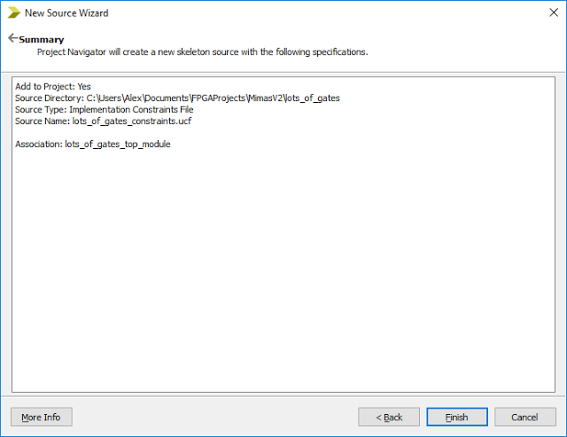
Click Finish to return to the main project screen. Now we need to decide how we want our DIP switches and LEDS to connect to our inputs and outputs.
Here is the code:
#++++++++++++++++++++++++++++++++++++++++++++++++++++++++++++++++++#
# This file is a .ucf for Mimas V2 #
# To use it in your project : #
# * Remove or comment the lines corresponding to unused pins in #
# the project #
# * Rename the used signals according to the your project #
#++++++++++++++++++++++++++++++++++++++++++++++++++++++++++++++++++#
CONFIG VCCAUX = "3.3" ;
#NET "CLK" LOC = V10 | IOSTANDARD = LVCMOS33 | PERIOD = 100MHz;
#NET "RST_n" IOSTANDARD = LVCMOS33 | PULLUP;
#################################################################################
# DIP Switches #
#################################################################################
NET "Not_input" LOC = C17 | IOSTANDARD = LVCMOS33 | DRIVE = 8 | SLEW = FAST | PULLUP;
NET "And_A_Input" LOC = C18 | IOSTANDARD = LVCMOS33 | DRIVE = 8 | SLEW = FAST | PULLUP;
NET "And_B_Input" LOC = D17 | IOSTANDARD = LVCMOS33 | DRIVE = 8 | SLEW = FAST | PULLUP;
NET "Or_A_Input" LOC = D18 | IOSTANDARD = LVCMOS33 | DRIVE = 8 | SLEW = FAST | PULLUP;
NET "Or_B_Input" LOC = E18 | IOSTANDARD = LVCMOS33 | DRIVE = 8 | SLEW = FAST | PULLUP;
NET "Xor_A_Input" LOC = E16 | IOSTANDARD = LVCMOS33 | DRIVE = 8 | SLEW = FAST | PULLUP;
NET "Xor_B_Input" LOC = F18 | IOSTANDARD = LVCMOS33 | DRIVE = 8 | SLEW = FAST | PULLUP;
#################################################################################
# LEDs #
#################################################################################
NET "Not_Output_LED" LOC = P15 | IOSTANDARD = LVCMOS33 | DRIVE = 8 | SLEW = FAST;
NET "And_Q_Output_LED" LOC = N15 | IOSTANDARD = LVCMOS33 | DRIVE = 8 | SLEW = FAST;
NET "Or_Q_Output_LED" LOC = U17 | IOSTANDARD = LVCMOS33 | DRIVE = 8 | SLEW = FAST;
NET "Xor_Q_Output_LED" LOC = T17 | IOSTANDARD = LVCMOS33 | DRIVE = 8 | SLEW = FAST;
Copy and paste the above code into the constraints file and then Save the file! It's now time to check everything is correct and implement everything before creating a bit stream file and upload it to the Mimas V2....
Click on the green arrow in the process window to process all of the code. Once complete there should be green tick marks on each section:

Next right click on Generate Programming File and Process Properties and select create Binary Configuration file:

Click Ok and then Right click on Generate Programming file and select run:

Once that has completed - connect up the Mimas V2 development board to your computer and load up the Mimas V2 Config tool. Select the correct COM port and finally navigate to the recently created Bit Stream file called 'lots_of_gates_top_module.bin' and click Upload:

It may take a while...I hear that programming the Mimas V2 using a JTAG programmer is considerably faster! Once that has completed lets test it out!
Remember that the Mimas V2 Logic levels are active low. So the LEDS will be off when a logic '1' is present at the output.
If people need access to the project and files it's here:
https://drive.google.com/open?id=0B7fA8ZgAyKMlaHo5Qms2YjhtNW8
That's all for now people - take care, Langster!

Associate the test bench source file with the code you wish to simulate...click Next when ready to continue:

Click finish to continue and return to the main project window:

Helpfully Xilinx WebISE has automatically generated the test bench code for us...unhelpfully it has also introduced some errors. Don't worry about these for now...the code generated is expecting a clock source to be present. There isn't a clock source in our design as we did not need one. We will remove the errors when we modify the test bench code. Again I like remove the top comments as I don't need them. Comments are useful but only when necessary...
Here is the code with the comments removed:
LIBRARY ieee;
USE ieee.std_logic_1164.ALL;

ENTITY Not_gate_tb IS
END Not_gate_tb;

ARCHITECTURE behavior OF Not_gate_tb IS

    -- Component Declaration for the Unit Under Test (UUT)

    COMPONENT Not_gate
    PORT(
         A : IN  std_logic;
         B : OUT  std_logic
        );
    END COMPONENT;


   --Inputs
   signal A : std_logic := '0';

  --Outputs
   signal B : std_logic;
   -- No clocks detected in port list. Replace <clock> below with
   -- appropriate port name

   constant <clock>_period : time := 10 ns;

BEGIN

 -- Instantiate the Unit Under Test (UUT)
   uut: Not_gate PORT MAP (
          A => A,
          B => B
        );

   -- Clock process definitions
   <clock>_process :process
   begin
  <clock> <= '0';
  wait for <clock>_period/2;
  <clock> <= '1';
  wait for <clock>_period/2;
   end process;


   -- Stimulus process
   stim_proc: process
   begin
      -- hold reset state for 100 ns.
      wait for 100 ns;

      wait for <clock>_period*10;

      -- insert stimulus here

      wait;
   end process;

END;
Now we need to remove the code relating to the automatically generated clock as this isn't
required:
LIBRARY ieee;
USE ieee.std_logic_1164.ALL;

ENTITY Not_gate_tb IS
END Not_gate_tb;

ARCHITECTURE behavior OF Not_gate_tb IS

    -- Component Declaration for the Unit Under Test (UUT)

    COMPONENT Not_gate
    PORT(
         A : IN  std_logic;
         B : OUT  std_logic
        );
    END COMPONENT;


   --Inputs
   signal A : std_logic := '0';

  --Outputs
   signal B : std_logic;

BEGIN

 -- Instantiate the Unit Under Test (UUT)
   uut: Not_gate PORT MAP (
          A => A,
          B => B
        );

   -- Stimulus process
   stim_proc: process
   begin
      -- hold reset state for 100 ns.
      wait for 100 ns;

      -- insert stimulus here

      wait;
   end process;

END;
The code generated actually uses the component statement so our automatically generated code is a perfect example of how a statement should be used! In the architecture statement we can see the component declaration for the Not_gate. Below that section some internal signals are defined to connect to the component we would like to simulate. Underneath that section we have the instantiation section which creates a version of the not_gate called 'uut' and maps the internal signal connections to the component signal connections. Now we need to write some code in the stimulus process section which sets the A input signal to a known value so that the simulator can run the code in the Not_gate module and display what will happen at the output signal - B.
As the module is an inverter or not gate it should be obvious that whatever logic level is present at the output signal is the opposite or inverse of the input signal. For more complicated modules this might be more difficult to assess which is why simulation is useful. It is also possible to see if there are any timing or sequencing issues present with more complicated modules. Simulation can be a very useful diagnostic tool when developing FPGA code.
Let’s write the stimulus VHDL code to test the module code and provide the simulator some information. Let’s set the 'A' input of the inverter to logic '1' for 100 ns and then set it to logic '0' for 100 ns and then set it to an unknown logic level 'X' for 100 ns. When we run the simulator we will be able to visually see what the output signal 'B' does when presented with those input 'stimuli' or logic states.
*Stimuli - a latin word which is the plural of stimulus, to provide a specific functional reaction!
Here is the code:
-- Stimulus process
   stim_proc: process
   begin
      -- hold reset state for 100 ns.
      wait for 100 ns;

      A <= '1';
  wait for 100 ns;

  A <= '0';
  wait for 100 ns;

  A <= 'X';
  wait for 100 ns;

      wait;
   end process;
Let’s save the code and run the simulator! Click on the Not_gate VHDL test bench module in the Hierarchy window:

Next right click on 'Behavioral Check Syntax' in the process window and select Run:

Once the process has completed there should be a green tick present:

Next right click on Simulate Behavioral Model and select Run:

Once the process has completed the ISIM screen will be displayed showing the results of the simulation:

At first it looks as though the simulation has failed as the result traces are red and in an X state - don't worry though that is what was expected. The last state we simulated was an 'X' state for the input signal. Click on the 'Zoom to Full View' icon on the toolbar to display the full results traces:

The green part of the traces show how the input 'A' went from a logic '0' to a logic '1' after 100 ns and the output 'B' changed accordingly. Then the input 'A' went from a logic '1' to a logic '0' for 100 ns and then the input 'A' was set to an unknown logic state 'X' and the output 'B' responded with a logic 'X' for the rest of the simulation - exactly what the test bench code was meant to do. So our simulation worked perfectly and more importantly the Not_gate module works perfectly!
This module can now be reused as many times as we like in any of our designs - Most Excellent!
Close down the ISIM application as we are finished with that program to return to the main project screen.
Let’s add some more logic functions like the AND, OR, and XOR functions. I'm not going to show all of the steps with pictures this time though, it's the same process as before.
Click on the implementation radio button and then add new VHDL source modules to the project. I called mine And_gate, Or_gate and XOR_gate. I chose to make them all two input devices with one output.

Here is the project window with all of the VHDL source file modules:

I deleted all of the comments that were not needed for each of the new modules and added the necessary code for the architecture sections. The code should be pretty self-explanatory but just in case here is the VHDL code for each logic function:
And Gate logic function VHDL code:
library IEEE;
use IEEE.STD_LOGIC_1164.ALL;
entity And_Gate is
Port ( A : in STD_LOGIC;
B : in
STD_LOGIC;
Q : out
STD_LOGIC);
end And_Gate;
architecture Behavioral of And_Gate is
begin
Q <= A and B;
Or Gate logic function VHDL code:
library IEEE;
use IEEE.STD_LOGIC_1164.ALL;
entity Or_gate is
Port ( A : in STD_LOGIC;
B : in
STD_LOGIC;
Q : out
STD_LOGIC);
end Or_gate;
architecture Behavioral of Or_gate is
begin
Q <= A or B;
Xor Gate logic function VHDL code:
library IEEE;
use IEEE.STD_LOGIC_1164.ALL;
entity Xor_gate is
Port ( A : in STD_LOGIC;
B : in
STD_LOGIC;
Q : out
STD_LOGIC);
end Xor_gate;
architecture Behavioral of Xor_gate is
begin
Q <= A xor B;
Ensure each VHDL module has the correct code. If you were so inclined you could then simulate each module to make certain the code behaves as intended. I'm not going to bother this time but for more complicated modules it's very important that it's simulated. I have saved myself hours of debugging by simulating the module behaviour before continuing.
At this point I like to draw a diagram which shows what function I want all of these modules to perform when connected together. Normally I would do this before I start writing the code but as this is just an example I'm doing it now. Lets implement each logic gate into the FPGA and use the DIP switches to connect to the inputs of the logic gates and then lets connect the outputs of the logic gates to the LEDS so that we can see the results when we change the state of the DIP switches!

From the diagram we can now create a VHDL top module which will connect to the DIP switches and LED and we can then make components to call all of the other modules and connect those modules inputs and outputs to the top module's inputs and outputs. Sounds complicated but it is actually fairly simple. Lets create the top module by right clicking in the hierarchy window as before...I called mine lots_of_gates_top_module:

Click Next and lets select how many inputs and outputs we will need. We need one input and output for the Not gate, two inputs and one output for the And gate, Or gate and Xor gate. So that makes seven inputs and four outputs. Give the inputs and outputs sensible names:

Click next to display the summary screen:

Click Finish to return to the main project screen.

Again remove the comments that are not necessary. Add comments later if required...

Now we need to add the component statements in the architecture section. The first
component we want to add is the Not gate. There is a really cool and easy way to do this thanks to Xilinx WebISE all we have to do is click on the module we want to use and then click on the Design Utilities option in the process window and double click on 'View HDL Instantiation Template':

We can then select and copy the code without the comments and paste it into the architecture section of the top module. It saves typing and it's completely correct! All we then need to do is correctly complete the port map section and our first component is done:

The Not_gate component signal connections map to the Not_input signal and the Not_Output_LED signal. I also changed the component instantiation label to something more meaningful. It can get awkward when you have multiple components of the same type if you don't use a sensible naming convention:

Repeat the process for all of the other components we intend to add. Once you have done that we need to move the instantiation sections to the begin and end section of the architecture statement. Once complete the code should look like this:
library IEEE;
use IEEE.STD_LOGIC_1164.ALL;
entity lots_of_gates_top_module is
Port (
Not_input : in STD_LOGIC;
Not_Output_LED : out STD_LOGIC;
And_A_Input : in STD_LOGIC;
And_B_Input : in STD_LOGIC;
And_Q_Output_LED : out STD_LOGIC;
Or_A_Input : in STD_LOGIC;
Or_B_Input : in STD_LOGIC;
Or_Q_Output_LED : out STD_LOGIC;
Xor_A_Input : in STD_LOGIC;
Xor_B_Input : in STD_LOGIC;
Xor_Q_Output_LED : out STD_LOGIC);
end lots_of_gates_top_module;
architecture Behavioral of lots_of_gates_top_module is
COMPONENT Not_gate
PORT(
A : IN std_logic;
B : OUT std_logic
);
END COMPONENT;
COMPONENT And_Gate
PORT(
A : IN std_logic;
B : IN std_logic;
Q : OUT std_logic
);
END COMPONENT;
COMPONENT Or_gate
PORT(
A : IN std_logic;
B : IN std_logic;
Q : OUT std_logic
);
END COMPONENT;
COMPONENT Xor_gate
PORT(
A : IN std_logic;
B : IN std_logic;
Q : OUT std_logic
);
END COMPONENT;
begin
Not_gate_1: Not_gate PORT MAP(
A => Not_input,
B => Not_Output_LED
);
And_Gate_1: And_Gate PORT MAP(
A => And_A_Input,
B => And_B_Input,
Q => And_Q_Output_LED
);
Or_gate_1: Or_gate PORT MAP(
A => Or_A_Input,
B => Or_B_Input,
Q => Or_Q_Output_LED
);
Xor_gate_1: Xor_gate PORT MAP(
A => Xor_A_Input,
B => Xor_B_Input,
Q => Xor_Q_Output_LED
);
end Behavioral;
The code should be fairly self-explanatory. Save the module and now let’s simulate it to make sure it will work as intended. Using the same process as before let’s create a test bench forthe top module and make sure that everything will work.
Click on the simulate radio button in the hierarchy window and then add a new source, select VHDL test bench and give it a suitable name. I called mine lots_gates_test_bench. Then associate the module with the lots_of_gates VHDL module and click finish. Then WebISE will generate some code for us. Delete the comments as necessary. After that delete the clock sections as we don't need those sections.
Finally all that is needed is to write the stimuli section like before. Lets exercise each gate in turn with suitable logic levels and allow time for each state to be easily viewed on the simulator screen. We could exercise all the gates at once but I prefer to see each state separately.
Here is the stimulus code:
library IEEE;
use IEEE.STD_LOGIC_1164.ALL;
entity lots_of_gates_top_module is
Port (
Not_input : in STD_LOGIC;
Not_Output_LED : out STD_LOGIC;
And_A_Input : in STD_LOGIC;
And_B_Input : in STD_LOGIC;
And_Q_Output_LED : out STD_LOGIC;
Or_A_Input : in STD_LOGIC;
Or_B_Input : in STD_LOGIC;
Or_Q_Output_LED : out STD_LOGIC;
Xor_A_Input : in STD_LOGIC;
Xor_B_Input : in STD_LOGIC;
Xor_Q_Output_LED : out STD_LOGIC);
end lots_of_gates_top_module;
architecture Behavioral of lots_of_gates_top_module is
COMPONENT Not_gate
PORT(
A : IN std_logic;
B : OUT std_logic
);
END COMPONENT;
COMPONENT And_Gate
PORT(
A : IN std_logic;
B : IN std_logic;
Q : OUT std_logic
);
END COMPONENT;
COMPONENT Or_gate
PORT(
A : IN std_logic;
B : IN std_logic;
Q : OUT std_logic
);
END COMPONENT;
COMPONENT Xor_gate
PORT(
A : IN std_logic;
B : IN std_logic;
Q : OUT std_logic
);
END COMPONENT;
begin
Not_gate_1: Not_gate PORT MAP(
A => Not_input,
B => Not_Output_LED
);
And_Gate_1: And_Gate PORT MAP(
A => And_A_Input,
B => And_B_Input,
Q => And_Q_Output_LED
);
Or_gate_1: Or_gate PORT MAP(
A => Or_A_Input,
B => Or_B_Input,
Q => Or_Q_Output_LED
);
Xor_gate_1: Xor_gate PORT MAP(
A => Xor_A_Input,
B => Xor_B_Input,
Q => Xor_Q_Output_LED
);
Let’s check the syntax and run the simulator!
Here is the result, I did manipulate the traces to put the outputs next to the inputs:

Close down the simulator...It’s time for the final bit of code writing - creating the implementation constraints file to tell WebISE how the external devices will connect to the FPGA signals in our design. In the hierarchy window click on add new source and choose implementation constraints file:


Click Finish to return to the main project screen. Now we need to decide how we want our DIP switches and LEDS to connect to our inputs and outputs.
- Let’s set DIP switch 0 to be the Not gate input
- Let’s set LED 0 to be the Not gate output
- Let’s set DIP switch 1 to be the AND gate A input
- Let’s set DIP switch 2 to be the AND gate B input
- Let’s set LED 1 to be the AND gate Output
- Let’s set DIP switch 3 to be the OR gate A input
- Let’s set DIP switch 4 to be the OR gate B input
- Let’s set LED 3 to be the OR gate Output
- Let’s set DIP switch 5 to be the XOR gate A input
- Let’s set DIP switch 6 to be the XOR gate B input
- Let’s set LED 5 to be the XOR gate Output
Here is the code:
#++++++++++++++++++++++++++++++++++++++++++++++++++++++++++++++++++#
# This file is a .ucf for Mimas V2 #
# To use it in your project : #
# * Remove or comment the lines corresponding to unused pins in #
# the project #
# * Rename the used signals according to the your project #
#++++++++++++++++++++++++++++++++++++++++++++++++++++++++++++++++++#
CONFIG VCCAUX = "3.3" ;
#NET "CLK" LOC = V10 | IOSTANDARD = LVCMOS33 | PERIOD = 100MHz;
#NET "RST_n" IOSTANDARD = LVCMOS33 | PULLUP;
#################################################################################
# DIP Switches #
#################################################################################
NET "Not_input" LOC = C17 | IOSTANDARD = LVCMOS33 | DRIVE = 8 | SLEW = FAST | PULLUP;
NET "And_A_Input" LOC = C18 | IOSTANDARD = LVCMOS33 | DRIVE = 8 | SLEW = FAST | PULLUP;
NET "And_B_Input" LOC = D17 | IOSTANDARD = LVCMOS33 | DRIVE = 8 | SLEW = FAST | PULLUP;
NET "Or_A_Input" LOC = D18 | IOSTANDARD = LVCMOS33 | DRIVE = 8 | SLEW = FAST | PULLUP;
NET "Or_B_Input" LOC = E18 | IOSTANDARD = LVCMOS33 | DRIVE = 8 | SLEW = FAST | PULLUP;
NET "Xor_A_Input" LOC = E16 | IOSTANDARD = LVCMOS33 | DRIVE = 8 | SLEW = FAST | PULLUP;
NET "Xor_B_Input" LOC = F18 | IOSTANDARD = LVCMOS33 | DRIVE = 8 | SLEW = FAST | PULLUP;
#################################################################################
# LEDs #
#################################################################################
NET "Not_Output_LED" LOC = P15 | IOSTANDARD = LVCMOS33 | DRIVE = 8 | SLEW = FAST;
NET "And_Q_Output_LED" LOC = N15 | IOSTANDARD = LVCMOS33 | DRIVE = 8 | SLEW = FAST;
NET "Or_Q_Output_LED" LOC = U17 | IOSTANDARD = LVCMOS33 | DRIVE = 8 | SLEW = FAST;
NET "Xor_Q_Output_LED" LOC = T17 | IOSTANDARD = LVCMOS33 | DRIVE = 8 | SLEW = FAST;
Copy and paste the above code into the constraints file and then Save the file! It's now time to check everything is correct and implement everything before creating a bit stream file and upload it to the Mimas V2....
Click on the green arrow in the process window to process all of the code. Once complete there should be green tick marks on each section:

Next right click on Generate Programming File and Process Properties and select create Binary Configuration file:

Click Ok and then Right click on Generate Programming file and select run:

Once that has completed - connect up the Mimas V2 development board to your computer and load up the Mimas V2 Config tool. Select the correct COM port and finally navigate to the recently created Bit Stream file called 'lots_of_gates_top_module.bin' and click Upload:

It may take a while...I hear that programming the Mimas V2 using a JTAG programmer is considerably faster! Once that has completed lets test it out!
- If you manipulate DIP switch 8 - the D1 LED will change state
- If you manipulate DIP switches 6 and 7 - the D3 LED will change state (AND function)
- If you manipulate DIP switches 4 and 5 - the D5 LED will change state (OR function)
- If you manipulate DIP switches 2 and 3 - the D7 LED will change state (XOR function)
 |
| The project uploaded to the Mimas V2 and working! |
Well that's about it for now...Apologies for the really long post. I couldn't really find a way to make it much shorter. If you want to be adventurous change the code to have multiple NOT gates, or AND gates etc....it only requires changing the instantiation sections with a single component declaration, you will need to map the pins though.
If people need access to the project and files it's here:
https://drive.google.com/open?id=0B7fA8ZgAyKMlaHo5Qms2YjhtNW8
That's all for now people - take care, Langster!