Thursday, 5 September 2019

ULX3S Open Source FPGA Development Board

I have made no secret of the fact that I am interested in FPGA technology and have been trying to relearn VHDL for some time.  I am also very keen on using open source programs and development tools.

Recently (sometime in the last couple of years) I heard about project IceStorm by Clifford Wolfe.  Mr Wolfe has reverse engineered Lattice Semiconductor's bit-stream files and written a software tool called Yosys which is used to convert verilog files into mapping files which can then be loaded onto a lattice semi-conductor FPGA.  At the moment proprietary FPGA development tools are very large pieces of software which take a lot of space on a hard disk, are feature heavy and not free to use (require licence files), often unsupported (Xilinx WEBise anyone) and I found difficult to use.  I'm not saying they aren't good but if I can use open source software tools I will...I like the idea behind the licensing models.  I'll donate what I can afford and assist wherever I can.

The Yosys Website is here: http://www.clifford.at/yosys/

Project ICE Storm: http://www.clifford.at/icestorm/

Until recently I didn't have a Lattice Semiconductor FPGA development board but that changed when I was offered a ULX3S open source board from the very clever guys at the Radiona Hackspace.  I had come into contact with these gentlemen when I was trying to learn to use the Elbert V2 and Mimas V2 Xilinx based FPGA development boards.  They developed a very cool piece of kit to make use of the open source tools for teaching a Digital Logic course at their local university.

The ULX3S with 3D printed case and buttons!
The board arrived in very good order with a 3D printed case, buttons and some pre-built examples.  I had a quick play with it and intended to write up my experiences and get started on using it.  That was probably this time last year...I am attempting to get back into blogging my experiences, trials and tribulations outside of work as I find it quite useful and I find it forces me to improve on my electronics and development skills.  Anyway...back to the board:

The board is in my opinion, very well designed and implemented.  I particularly like the addition of the ESP32 so files can be uploaded over wifi.

Here are some photos of the board:

The top side of the PCB with buttons, microSD card and display
The underside of the PCB with the ESP32 module
Here is the website for the project: https://radiona.org/ulx3s/

Here is a Hackaday write up: https://hackaday.com/2019/01/14/ulx3s-an-open-source-lattice-ecp5-fpga-pcb/#more-340565

I'll be honest, I bought the board to support the project, I haven't got a project or use in mind.  To be even more honest I still want to re-learn a hardware description language so that when I do have a project in mind I'll be able to make use of the technology.  I do have ideas for a piece of instrumentation but that is a way off and requires a lot more than just the FPGA!

The first thing I did with the board was use it to emulate an Amiga 500 computer using the pre-loaded Minimig project which came ready to play on the board.  All I had to do was grab some amiga disk images and I could play all the games from my misspent youth.  Retro gaming with FPGA devices is a very popular hobby as the hardware is not being emulated but actually realised within the fabric of the device which leads to a more realistic experience.

Playing Lotus Turbo Challenge 2 and Utopia are fun diversions but not quite what I had in mind for the device.

The open source tools all appear to be for linux operating systems only at the moment so I installed Linux Mint on my main PC and got to work installing all of the pieces of software needed from project Ice storm.  

My LinuxFu is not that strong so I may have messed this up somewhere along the way.  I know I have downloaded, and compiled the following pieces of software:

IceStudio
prjtrellis
Yosys
nextPNR

I was then pointed towards the apio project by a colleague and downloaded the windows version of that software along with all the other bits and pieces needed by following the instructions here:

https://github.com/ulx3s/fpga-odysseus

It installed fine although I would ensure that if following the instructions that you don't upgrade the apio software.

Once presented with the command prompt by loading the ConEmu.exe program it is pretty easy to get started:


This screen brought my back to my days of the DOS prompt.  I know the linux command prompt is fairly similar but I just don't use linux enough to be comfortable with it...I am slowly improving though...

I made a folder called Alex and then a sub folder called ulx3s, you could use any folder names you like.  I then copied two files into the folder:

apio.ini - found from the folder C:\msys64\src\fpga-odysseus\tutorials\01-Basics\01-LED
ulx3s_v20.lpf - found from the folder C:\msys64\src\fpga-odysseus\tutorials\01-Basics\01-LED

The apio.ini file is a text file that tells the apio software everything needed to prepare files for upload to the ulx3s board and ulx3s_v20.lpf is the constraints file for the board, it tells apio and all of the other software which pins are connected to what and where between the FPGA and the external peripherals.

I next created a simple text file in notepad++ - you could use any text editor to be honest.  I called it top.v and typed out the following simple program:

//Hello world LED program

//create a module called top
module top (
    output [7:0] led, //create an output vector called 'led' with 8 bits
    output wifi_gpio0 //create an output for the wifi gpio
);
    assign led = 8'b10101010; //set the state of the bits in the vector to the number 170
 // this sets the bits on and off alternately

    assign wifi_gpio0 = 1'b1; // set the wifi gpio wifi high 
endmodule //end the module

Save the file in the directory made previously:

C:\msys64\src\Alex\ulx3s

Next jump to the ConEmu command prompt and make sure all of the files we need are there by typing ls and hit enter :


next type the following: apio build --board ulx3s-45f'

You should see the following displayed, ignore the warning messages:


  The following files will have been created in the directory:

Exciting times....now it is time to upload the program to the FPGA.  Make sure the ULX3S board is plugged into a suitable USB port and powered up.

Type the following command:

apio upload --board ulx3s-45f

If all goes according to plan you should see the following:


Next type the following:

apio clean

This removes all of the unnecessary files created during the processes.  Finally its time to admire your work.  If everything went according to plan you should see the following LED pattern on your ULX3S!


Ok so its nothing special but it's a start. I'm hoping soon to do a bit more with it.  I hear good things about something called ICE Studio:

https://icestudio.io/

It doesn't have support for the ulx3s yet but I'm hopeful it can be added soon!

That's all for now - Langster!

Sunday, 28 July 2019

Finishing off the Interactive Confetti Room Controller

Last week I managed to help finish off the interactive confetti room controller.  It which was finally made up of the following components:

1x Arduino Uno R3 clone
1x prototyping shield
1x magnetic door sensor and complementary magnet
3x 10 kΩ resistors
1x DS1307 i2c real time clock module
1x Elegoo 8 channel relay module
5x Single UK mains plug socket extensions
1x 5 Vdc power supply for the Arduino Uno and Relay PCB

The build was put together as follows:


The mains power all came from a single input poorly shown coming in at the bottom left.  This connection was then used to power the 5 Vdc power supply for the arduino and the relay module.  The live connection to the outputs was controlled by the relay PCB between the normally open and common connections.  The relays inputs were connected to the arduino uno digital pins at 11, 10, 9 and 8 respectively.  The door sensor was connected via between 5 Vdc and digital pin 2 of the arduino, a 10  resistor and GND.  The real time clock module was connected to the i2c pins A4 and A5 of the arduino UNO.  The i2c lines were also 'pulled up to 5 Vdc via 10 kΩ resistors to ensure correct operation.  

Note: The Elegoo relay module screw terminals are quite small and it was difficult to insert 1.5 mm diameter mains cable into them.  I ended up getting some thick single core house wiring conductor and using that and when connecting the live conductor to that.  I then covered the lot in hot glue and insulating tape to try to prevent the exposed live being touched.  As everything is going inside a box it shouldn't be an issue anyway.  The final user who will be using this controller and developing the firmware was clearly warned!  

The whole assembly was mounted to a laser cut wooden baseboard...as this turned out to be a little undersized I then put the whole lot inside a 230 x 230 x 120 mm laser cut wooden box.  Strain relief was added to all cables using some cable ties. The lid was left off while the firmware was developed by the customer.  I assisted where I was requested but I am not the best at coding and was also short on time so I left them to it!

Here is a photo of the kit inside the box:


Here is a photo of the box with it's unattached lid:


Well that's it for this quick project.  I may well add source code and video of the final effect when I get the chance to see it!  I'm aware this post lacks the usual detail but there wasn't much to write about.

That's all for now - Langster!

Sunday, 7 July 2019

Elegoo 8 Channel Relay Module Tutorial

Carrying on from the previous post about an interactive confetti room...

https://langster1980.blogspot.com/2019/07/interactive-confetti-room-project.html

Lets get out the 8 channel relay PCB and see what makes it tick.

Here are the specifications of the device in case it is needed:

● Output Channels: 8
● Operating Voltage: 5 Vdc
● Operating Current: 480 ma
● Switching Voltages: 250 Vac at 10 Amps, 30 Vdc at 10 A

● Mechanical Dimensions (Length*Width*Height): 137 mm x 56 mm x 17 mm (5.4" x 2.2" x 0.7")
● Mounting Hole Size: 3 mm (0.12")
● Mounting Hole Centres (L*W): 132 x 50 mm (5.2" x 2")

Here is the schematic diagram again:


I connected up the relay board to the Arduino R3 as shown in the diagram below:
This connection arrangement will actuate the channel 1 relay switching the positive feed (+5 Vdc) on it's common and normally closed connections.  Anything connected between the common pin and the normally closed pin will be switched, It could be anything as long as it is within the specifications of the relay contacts.  The normally open pin will also be switched as the common pin is in the middle of the switching contacts.

We want to write some simple test code to drive the relay coil on channel one on and off for a brief period of time:

1.  Initialise control variables
2.  Start the Serial Monitor
3.  Set the relay drive pins to be outputs
4.  Open channel 1 relay contacts
5.  Wait half a second
6.  Close channel 1 relay contacts
7.  Loop back to step 4 and repeat continuously

Here is the code:

/* Langster's Test Code for 
 *  Elegoo 8 Channel Relay PCB
 *  07/07/2019
 *  Test circuit output is a Green 5 mm LED 
 *  and a 220 Ohm resistor connected
 *  between common and Normally Closed screw
 *  terminals on the channel 1 relay outputs
 *  
 *  The Elegoo relay module is connected to
 *  an Arduino Uno R3 on the following pins:
 *  
 *  GND connects to GND of the Arduino
 *  IN1 connects to Pin 11 of the Arduino
 *  IN1 connects to Pin 10 of the Arduino
 *  IN2 connects to Pin 9 of the Arduino
 *  IN3 connects to Pin 8 of the Arduino
 *  IN4 connects to Pin 7 of the Arduino
 *  IN5 connects to Pin 6 of the Arduino
 *  IN6 connects to Pin 5 of the Arduino
 *  IN7 connects to Pin 4 of the Arduino
 *  VCC connects to Vin pin of the Arduino
 */

int eightChanRelayIN1 = 11;   //variable for relay channel 1 drive pin
int eightChanRelayIN2 = 10;   //variable for relay channel 2 drive pin
int eightChanRelayIN3 = 9;   //variable for relay channel 3 drive pin
int eightChanRelayIN4 = 8;   //variable for relay channel 4 drive pin
int eightChanRelayIN5 = 7;   //variable for relay channel 5 drive pin
int eightChanRelayIN6 = 6;   //variable for relay channel 6 drive pin
int eightChanRelayIN7 = 5;   //variable for relay channel 7 drive pin
int eightChanRelayIN8 = 4;   //variable for relay channel 8 drive pin

int relayDwellTimeMS = 500; //variable for setting the dwell time a relay is actuated for

void setup() {

Serial.begin(9600);      // open the serial port at 9600 bps:
pinMode(eightChanRelayIN1, OUTPUT); //set the relay drive pin for channel 1 to be an output
pinMode(eightChanRelayIN2, OUTPUT); //set the relay drive pin for channel 2 to be an output
pinMode(eightChanRelayIN3, OUTPUT); //set the relay drive pin for channel 3 to be an output
pinMode(eightChanRelayIN4, OUTPUT); //set the relay drive pin for channel 4 to be an output
pinMode(eightChanRelayIN5, OUTPUT); //set the relay drive pin for channel 5 to be an output
pinMode(eightChanRelayIN6, OUTPUT); //set the relay drive pin for channel 6 to be an output
pinMode(eightChanRelayIN7, OUTPUT); //set the relay drive pin for channel 7 to be an output
pinMode(eightChanRelayIN8, OUTPUT); //set the relay drive pin for channel 8 to be an output

}

void loop() {

digitalWrite(eightChanRelayIN1, LOW);   //switch relay channel 1
delay(relayDwellTimeMS);                //wait for the dwell time (500 ms)
digitalWrite(eightChanRelayIN1, HIGH);  //switch relay channel 1
delay(relayDwellTimeMS);                //wait for the dwell time (500 ms)
 
}

The code is fairly easy to understand.  Each relay channel has been assigned a variable to easily reference it.  A variable to select how long the relay will be open or closed is also added, commonly known as the dwell time.

Next in the setup function the serial terminal is initialised although it isn't actually used for anything (I had plans to add serial messages and then didn't bother).

After that all the relay channel drive pins are set to outputs. 

Finally in the loop function the relay on channel one is driven low which opens it's contacts.  The contacts stay open for half a second and then the contacts are closed - the pin is driven high for half a second and then the function loops back to the start and repeats.

Here is a short video of things in action:


Things to note - The relay drive pins are active low. That means in order to make a relay switch the contact open the drive pin must be driven low.

It would not be difficult to modify the code to drive all of the relays, just modify the code in the loop section:

void loop() {

  digitalWrite(eightChanRelayIN1, LOW);    //switch relay channel 1
  digitalWrite(eightChanRelayIN2, LOW);    //switch relay channel 2
  digitalWrite(eightChanRelayIN3, LOW);    //switch relay channel 3
  digitalWrite(eightChanRelayIN4, LOW);    //switch relay channel 4
  digitalWrite(eightChanRelayIN5, LOW);    //switch relay channel 5
  digitalWrite(eightChanRelayIN6, LOW);    //switch relay channel 6
  digitalWrite(eightChanRelayIN7, LOW);    //switch relay channel 7
  digitalWrite(eightChanRelayIN8, LOW);    //switch relay channel 8
  
  delay(relayDwellTimeMS);                 //wait for the dwell time (500 ms)
  
  digitalWrite(eightChanRelayIN1, HIGH);   //switch relay channel 1
  digitalWrite(eightChanRelayIN2, HIGH);   //switch relay channel 2
  digitalWrite(eightChanRelayIN3, HIGH);   //switch relay channel 3
  digitalWrite(eightChanRelayIN4, HIGH);   //switch relay channel 4
  digitalWrite(eightChanRelayIN5, HIGH);   //switch relay channel 5
  digitalWrite(eightChanRelayIN6, HIGH);   //switch relay channel 6
  digitalWrite(eightChanRelayIN7, HIGH);   //switch relay channel 7
  digitalWrite(eightChanRelayIN8, HIGH);   //switch relay channel 8
  
  delay(relayDwellTimeMS);                //wait for the dwell time (500 ms)
 
}

I haven't got eight LEDS to hand to give a demonstration of this but I have tested the code and the circuit it works perfectly...the clicking of the relays sounds a lot like an old fashioned watch tick or a metronome.

If one were to change value in the dwell time variable the relays will switch more quickly or slowly...the maximum speed they should be switched is 100 ms...any faster will work but might damage the relays and the noise is exceptionally irritating! 

The code can also be modified to independently switch each relay with independent dwell times as required. 

That's about it for now, take care - Langster!

Thursday, 4 July 2019

Interactive Confetti Room Project

I was recently asked to help develop the electronics for an event.  The basic idea is that people would enter a room filled with different coloured confetti and air blowers.  These air blowers would be energised for short periods of time in prescribed sequences blowing the confetti about the room in a colourful display.  Hopefully a little bit reminiscent of a final game in a classic British TV program - the Crystal Maze!  If people aren't aware of the cult classic of the crystal maze then a link is below:


The part I'm referring to is this, don't watch all of it! - skip to 2:17 for the important bit:


Hopefully people reading this post will get what I mean.  Anyway...in order to create a similar effect Five air blower units will be sourced and placed inside a 15 mroom.  The fan units will be placed in the corners with one unit in the mid point in effort to ensure there is some form of uniform airflow.  The coloured confetti is placed in front of the fan units and when people enter the room and the door is closed the fans will come on in a prescribed sequence creating an atmospheric effect.  This hasn't been tried and tested yet so some development of the experience may be required...I'll probably leave that part to others as I haven't the time and to be honest I have only been asked to help develop the kit not the experience...I'll help out where I can but getting the desired effect is up to the customer...I'll provide the tools not the results...

The above diagram hopefully gets the general idea across.

The fan blower units have already been selected and are linked below:


Vacmaster Air Mover | High Power, Energy Efficient Turbo Fan/Blower/Dryer
Image Credit - Vacmaster, via Amazon.co.uk
The specifications given via the Amazon product page are:

  • POWERFUL AIR FLOW - The 150 W motor drives 266 litres of ambient air per second for rapid drying and cooling.
  • ENERGY EFFICIENT - Consumes 90% less power than a conventional 1000 W fan heater.
  • 3 TILT POSITIONS - Tilts at 45 degrees, horizontally and vertically for precise, focused air flow.
  • 3 POWER SETTINGS - Low, medium and high speed settings for quiet or fast drying.
  • INTEGRATED EXTENSION SOCKET - For powering additional Air Movers from a single wall socket. Daisy-chain them together to cover a large area.
The vendor doesn't mention the mains supply voltage required but as this is the UK and it's being sourced via amazon UK I'm going to assume the supply is 230 Vac.  The current draw will therefore be 0.65 Amps - as Current (Amps) = Power (Watts) / Volts from Ohms Law:

150 Watts / 230 Vac = 0.6521739130434782608695652173913‬ Amps
or 0.65 Amps to two significant figures...

Lets write some requirements:

  • Switch five fans on and off independently in a pre-arranged sequence
  • Choose specific times of day when fans will come on and off
  • Ensure fans can only actuate when the door to the room is closed.
  • Ensure fans have independent overrides for safety - be able to turn fans on/off via control buttons
  • The switching requirement is 230 Vac at 0.65 Amps for each fan 

There are several ways this could be achieved.  As time is of the essence...as it always seems to be, I'm going to use relays to switch the mains feed to the fans.  The relays will be controlled via a microcontroller which can be communicated with using a serial terminal or via the buttons which will be on the front panel of the control unit.  If necessary I'll add an indication LED and maybe a buzzer to show when the fans are about to begin operation...I suspect the fan noise will make that clear to all concerned though - 😃

I could design my own relay control PCB complete with drive electronics or I could make use of a pre-made module...again time and budget suggests I go with something off the shelf.  I need a five channel relay module capable of switching 230 Vac at 0.65 Amps. I found this module on Amazon.co.uk and it looks to have everything needed...that'll save some time!

Elegoo 8 Channel Relay Module - via Amazon.co.uk

Image Credit - Elegoo 8 channel Relay Module via Amazon.co.uk
There are eight relays are capable of switching 230 Vac at 10 Amps - far more than we need and they meet the switching requirements.  They can be driven from 5 Vdc which means that they can be driven from a five volt tolerant microcontroller output.  The relay drive coils are optically isolated so the microcontroller won't be affected by the relay switching.  There is an LED (light emitting diode) at each relay channel to display when the relay coil is being driven.  The cost was a very reasonable GBP £8.99 or USD $11.31 which I would struggle to compete with if I were to design my own version.

The schematic diagram for the relay module is here in case it is needed:

We will also need the following components:

An arduino uno R3 microcontroller or clone - Via Amazon.co.uk
Some Momentary Buttons  - via Amazon.co.uk
Some jumper wires - via Amazon.co.uk
Some tri-colour LEDS - via Amazon.co.uk
Some LED holders - via Amazon.co.uk
Six mains sockets and wire - via Amazon.co.uk
Some connector block - via Amazon.co.uk
A reed switch and magnet - via Amazon.co.uk
A power supply for the Arduino - via Amazon.co.uk

The current plan (always subject to change) is to connect all the above components as follows:


Please excuse the crudeness of the diagram...I didn't have time to sort everything as much as I would have liked but it gets the general idea across...I've missed off the power supply to the arduino.  It is also connected to the incoming mains and then to the dc input socket on the arduino.  Not all of the relays need to be controlled by the arduino so some of the wires can be omitted as necessary and finally the reed switch should have a 10 k resistor pulling it down to 0 Vdc as with the buttons so that it is properly detected by the microcontroller input.

That's enough for now.  The next post will be on testing and using the Elegoo 8 channel relay module.

Take care, especially with mains wiring - Langster!

Thursday, 20 June 2019

How to Drive a Solenoid from a Microcontroller

I haven't posted anything in a long time...I just haven't been motivated enough to do so.  I suppose it could be because I'm busy but its more likely I've just lacked the energy to do anything.

I recently designed a simple FET driver circuit for energising a solenoid.  It wasn't particularly special in my opinion but I thought it might be useful to share the experience so here goes:

I had to drive a solenoid based circuit for an electronic lock from a microcontroller.  As a solenoid is essentially an inductive load I would need a transistor based circuit to control the supply voltage from a 3.3 Vdc signal generated by an STM32 microcontroller.  In order to actuate the solenoid a short pulse (less than a second) was required from a 12 Vdc or 24 Vdc supply.

A solenoid is an electro-magnetic actuator which creates a concentrated magnetic field.  Here are a couple of links about solenoids and how they work:

https://sciencing.com/a-solenoid-work-4567178.html

https://en.wikipedia.org/wiki/Solenoid

A simple switching circuit is all that is required to energise the solenoid coil and actuate it.  Electronic switching can be performed in many ways - a relay switch in itself is a form of electro-magnetic actuator.  In my case I decided to use a Field Effect Transistor or FET.  I've blogged about field effect transistors in the past:

https://langster1980.blogspot.com/2012/09/using-field-effect-transistors.html

The same principles apply.  Recently I read an excellent blog post by James Lewis - 'The Bald Engineer' on some of the misconceptions about using field effect transistors...I recommend looking at James's website.  He writes some excellent articles and makes some great video content on electronics engineering.

https://www.baldengineer.com/7-mosfet-myths-and-misconceptions-addressed.html#more-7748

As I had to drive the field effect transistor directly from a microcontroller pin at 3.3 Vdc I needed what is known as a logic level FET - That is a device that will allow current to flow between the drain and the source pins when the gate pin is supplied with logic level voltages, logic level voltages are normally classed as 1.8 Vdc, 3.3 Vdc and 5 Vdc.  In the case for the microcontroller I am using - an STM32F439 a logic 1 (high) is 3.3 Vdc.  Therefore I needed a FET which had a VGS on threshold that was at or below 3.3 Vdc.  I chose to use the IRLZ44 as I had some of those components and I also had a spice model for them so I can simulate the circuit.

From some brief measurements of my solenoid I found that it had a series resistance of about 33 ohms and I guessed it's inductance at 3 Henrys....I didn't have my LCR meter to hand to measure it....I might dig that out later to see what the inductance actually is.

Here is the datasheet for the IRLZ44: http://www.irf.com/product-info/datasheets/data/irlz44n.pdf

I'm using the T0220 version for my circuit:

Image result for IRLz44

The critical parameters I was interested in are:

VDSS = 55 Vdc - The maximum voltage allowed on the drain pin with respect to the source pin.

RDS(on) = 0.022 Ω - The resistance of the drain with respect to the source pin when the transistor is on.

ID = 47 Amps - The maximum current allowed to flow from the drain to the source.

VGS On Threshold = 2.0 Vdc - The voltage at which the FET turns OFF - Thanks James, I always wrong about this too!  This means in order to turn the FET on (cause conduction between the drain and source pins we need to surpass this this voltage at the gate pin.  If the voltage at the gate pin drops below this voltage the transistor will stop conducting from the drain pin to the source pin.  The parameter name is a little confusing but hey ho...

So what does this all mean.  It means that I can turn the transistor on using an output pin from a
3.3 Vdc microcontroller and that will allow conduction through the drain pin to the source pin which will allow me to control the voltage supplied to the solenoid.

Here is the circuit:

Simple Solenoid Driver Using a Logic Level FET
Here is the circuit's operation.  A 3.3 Vdc pulse will be supplied from the microcontroller.  This pulse is applied to the gate of the IRLZ44 FET through a 270 Ω resistor (R2).  The resistor R2 is present to prevent a large in-rush current being presented to the gate pin of the FET.  It isn't always necessary if one is only applying long slow voltage pulses to the gate.  I always add a resistor as I like to be certain there will not be any in rush current issues.  The 10 kΩ resistor (R1) is a pull down resistor.  It ensures that the gate pin of the IRLZ44 when not driven from the microcontroller is in a known state - low.  It prevents the FET from spuriously switching on or off.  The drain of the FET is connected to the solenoid (modelled in this case by the 33 Ω resistor and the 3 H inductor.  The schottkey diode (D1) is present to prevent the back-emf generated by the inductive load switching on and off damaging the FET.  D1 is sometimes called a 'free wheel diode' or the 'flyback' diode....More on this later.
 
The voltage source VCC and switch S1 are not really present but a way of simulating what the output from the microcontroller will be. If S1 is closed for a short period the signal presented to the gate pin will be similar to the output pulse from the microcontroller.  This pulse voltage will cause the FET to become active allowing current to flow from the drain to the source which in turn will allow voltage to flow through the solenoid causing it to actuate (create a magnetic field which pulls the pin into the coil).

If we were to simulate the operation of the circuit and observe the input and the output with an oscilloscope connected as shown above this is what would be seen:


The red trace is the the solenoid operation and the blue trace is the input from the microcontroller - modelled in this case by the switch S1 and the 3.3 Vdc voltage supply.

So our circuit simulates will and will work.  The FET operates properly from a 3.3 Vdc supply and can go active within a milli-second.  More than adequate for our purpose!

The only thing left I wanted to discuss was the flyback diode D1...it's needed as when an inductive load has voltage and current applied it converts the electrical energy into magnetic energy creating a concentrated magnetic field.  When an inductive load is has the voltage and current removed the magnetic field collapses and any left over energy is passed back to the drive circuit as a large voltage spike.  This spike is often well over 100 Volts for a short period - more than enough to damage the Field Effect Transistor.  Therefore the flyback diode is applied to prevent this damaging voltage spike passing to the FET.

To illustrate the point here is a circuit with a switch added to the flyback diode.  As the switch is open the diode is not connected.  When the magnetic field collapses this is what is passed back to the FET:


Here is the oscilloscope trace:


If the flyback diode was not present in the circuit the FET would fail fairly quickly...

I'll add some photos of the circuit I built shortly to show it in operation.  It works perfectly for my application.  Take care people - Langster!


Here is a quick video of the circuit on a bread board.  It was driving an electronic lock using 5 Vdc as the gate voltage:


Monday, 12 March 2018

AD9850 Signal Generator

I have a bit of free time at the moment and I was looking at previous projects and what equipment I have available to me.

I have couple of bench power supplies, an oscilloscope, a multimeter and a good stock of components for development.  I still don't have a Signal generator!  In previous posts I wrote about how I developed some addon circuitry for an AD9833 breakout board.  I never actually finished that project and I have since decided that there are better DDS signal generator breakout boards available.  I bought an AD9850 breakout board from a maker-faire vendor at least two years ago and it has sat in my breakout boards pile for a long time!

The breakout board is based on the AD9850 from Analog Devices and it's a DDS synthesis circuit.  The datasheet for the device is here:

http://www.analog.com/media/en/technical-documentation/data-sheets/AD9850.pdf

There are lots of tutorials and information available on the internet for how this device works and can be used to make a simple signal generator.  Some of the links I used for reference are below:

http://telecnatron.com/modules/ad9850/index.html

http://kv4qb.blogspot.co.uk/2017/04/the-sa-becomes-sna-jrv3-for-now.html

The number of projects and posts available for this board and how to use it are a testament to how good the device is and how easy it should be to use and get it up and running.  I may yet build a simple scalar network analyser with one to allow for filter and amplifier testing at some point.

For now I just need access to a signal generator.  I should have finished the one I designed years ago or bought one off the shelf!  The off the shelf devices that I see are all still quite expensive and don't have all of the functions I need.  I could probably find one that did meet all of my requirements if I looked hard enough and was prepared to part with a little more money!  The module itself costs £15.00 from various online vendors although I'm certain I paid less for it than that.


Here is the schematic diagram for the AD9850 breakout board:


As can be seen there is a filtered and unfiltered output.  Obviously we want to use the filtered output and see what comes out of the unit.

By connecting the unit up to an arduino and using example code we should be able to get the unit up and generating signals.  From that we can design an amplifier and match the circuit to 50 ohms and hopefully put together a useful piece of test equipment in short order!

Helpfully there are several libraries already written for driving the module using an arduino so that saves some time and effort:

https://github.com/F4GOJ/AD9850

Here is how the module is connected up for testing with an arduino mega:

AD9850 breakout board connected to an Arduino Mega
For connecting up the AD9850 module:

Pin 1 (Vcc), connect to the arduino +5V pin
Pin 2 (W_CLK), connect to the arduino digital pin 8
Pin 3 (FQ_UD), connect to the arduino digital pin 9
Pin 4 (Data), connect to the arduino digital pin 10
Pin 5 (Reset), connect to the arduino digital pin 11
Pin 6 (GND), connect to the arduino GND pin

Pin 10 (Filtered Sine Out), connect to an oscilloscope for testing

Here is the code I used to test the module:

 // Langster's DDS test Code  
 // Date: 12/03/2018  
 // Makes use of m0xpd's DDS Arduino Library  
 // http://m0xpd.blogspot.com  
 // include the DDS Library:  
 #include <DDS.h>  
 // AD9850 Module is connected to the following  
 // arduino pins  
 const int W_CLK = 8;  
 const int FQ_UD = 9;   
 const int DATA = 10;  
 const int RESET = 11;  
 double freq = 0;  
  // Instantiate the DDS...  
  DDS dds(W_CLK, FQ_UD, DATA, RESET);  
 void setup() {  
  // start up the DDS...    
  dds.init();   
  // (Optional) change value if the clock crystal does not resonate at 125MHz...  
  dds.trim(125000000); // enter actual oscillation frequency   
  // start the oscillator...  
  dds.setFrequency(freq);   
 }  
 void loop() {  
  dds.setFrequency(1000); //set the frequency output to 1 kHz   
 }  

The code will initiate the DDS module and then set an output of 1 kHz.

I connected up the filtered sine output to an oscilloscope and here is the result:

1 kHz sine output from Ad9850 DDS Module
A nice clean 1 Vpk to pk, 1 kHz sine wave!  The square wave output was also present and in good shape.  I'm going to perform more testing to check the useable frequency range but so far so good.

By changing the value in the line:

dds.setFrequency(1000); //set the frequency output to 1 kHz

The frequency output is changed.

That's all for now - Langster!

Sunday, 17 September 2017

Pulse Oximeter Functionality for a Medical Device

It has again been some time since I did any work on the medical device I have been developing, I've as usual, been busy!  The previous post is here in case it is of interest:

http://langster1980.blogspot.co.uk/2017/06/myoware-muscle-sensor-circuits-from.html

The gentlemen for whom I'm developing this hardware for has requested some additional functionality. The additional functionality requested is a Pulse Oximetry measurement.  Pulse Oximetry is the measurement of a person's pulse along with how much oxygen is present within their blood.  It is a common measurement made by medical practitioners to ensure their patients are in good health.  I suspect for the medical device, this information will be correlated with a person's breathing to assess how well a person's lungs are working and how much oxygen from the air is getting into their blood.

Image by Nonin Medical - http://www.nonin.com/What-is-Pulse-Oximetry
Here is an article by Nonin Medical on Pulse Oximetry:

http://www.nonin.com/What-is-Pulse-Oximetry

Here is the wikipedia article on Pulse Oximetry:

https://en.wikipedia.org/wiki/Pulse_oximetry

Here is another article on Pulse Oximetry:

https://www.howequipmentworks.com/pulse_oximeter/

The measurement works by shining a bright light through the a suitable point on the patient's skin and detecting the diffused light and from that the pulse and oxygen levels can be calculated.  The units used are SPO2 which stands for Peripheral Oxygen Saturation where:

SP = Peripheral saturation
O2 = Chemical symbol for an Oxygen molecule

There is a formula associated with Pulse Oximetry:
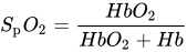


Where HbO2 is Oxygenated Haemoglobin and Hb is Deoxygenated Haemoglobin*

SPO2 is presented as a percentage and most people in normal conditions exhibit 94 to 99% saturation of oxygen in their blood.  If a person were unwell due to breathing difficulty then their SPO2 is lower.  If a person's SPOis below 65% then their ability to think clearly is impaired and if below 55% most people have lost consciousness.

*Haemoglobin is the red coloured metallo-protein within human blood which contains iron and carries oxygen around the body.

So that is the theory!  Lets talk about how one might design an electronic circuit to measure a person's SPO2 level.  We need to shine a light through an exposed part of the patient's skin say on the top of their index finger and measure the amount of light present at the bottom of the finger after the light has travelled through their skin.  At the same time the light signal needs to be converted to an electrical signal and then filtered.  It then will probably need to be amplified and finally converted from an analogue signal to a digital signal for processing by a microcontroller and finally displaying the resulting measurement.

It is not a particularly difficult circuit to design and plenty of other people have already done so.  I have put some of the sites I used as research below for interest:

https://www.swharden.com/wp/2013-04-14-simple-diy-ecg-pulse-oximeter-version-2/

http://www.instructables.com/id/Simple-DIY-Pulse-Sensor/

http://www.elektroda.pl/rtvforum/topic1655378.html?l=en

I may yet design my own implementation as it could be one way to reduce costs.  There is an Arduino R3 shield available though and it's open source.  It is made by ProtoCentral and is called the Proto Central AFE4490 Pulse Oximeter Shield V2.  It cost £71.12 which I actually think is a bit expensive however it does look to be well designed and implemented.

Image Credit - ProtoCentral AFE4490 Pulse Oximeter Shield for Arduino - v2
It can be bought from their website below:

Pulse Oximeter Arduino Shield

Because the device is completely open source (Very cool - I whole heartedly approve) the schematic is below:
The whole circuit is based around a very clever integrated circuit by Texas Instruments - the
AFE4490. The datasheet for this device is here:

http://www.ti.com/lit/ds/sbas602h/sbas602h.pdf

Basically the optical signal from the supplied finger clip connects to the nine way 'D type' connector on the Arduino shield. The signal output is protected from being too high by the the circuit labelled 'Protection circuit'  The diodes ensure that the electrical signals passed to and from the clip can never be greater than 3.3 Vdc which ensures that no damage can occur.

The analogue signal sent from the clip is processed by the AD4490 device which is a complete analogue front end device for pulse oximetry.  The device provides the electrical signals to drive the sensor clip, a 22 bit analogue to digital converter to change the analogue signal output from the sensor to a form which can be easily read into a microcontroller using the Serial Peripheral Interface (SPI) protocol.

The next part of the circuit is a simple power supply regulator from 5 Vdc to 3.3 Vdc with some filtering to prevent electronic noise from the Arduino R3 affecting the measurement circuitry.

A logic level converter device is present to ensure that the 3.3 Vdc signals from the AD4490 device are turned into 5 Vdc so that they are correctly read into the arduino and processed appropriately. There are two FET logic level converter circuits present to convert the 3.3 Vdc LED diagnostic signals to 5 Vdc for processing by the Arduino.

The final section shows how all the connections on the Shield connect to the Arduino R3.

The circuit looks to be exactly how one would use the AD4490 having read the datasheet in it's entirety.  Reading and understanding or interpreting datasheets is a true skill needed for aspiring electronics design engineers.

ProtoCentral have very helpfully provided example code which can be downloaded from their github site:

https://github.com/Protocentral/AFE4490_Oximeter/tree/master/arduino

I've uploaded the text only code to my arduino R3.

Lets see the circuit in action!


Here is the serial output:


Well there we have it - I'm alive, my blood is well oxygenated and my heart is beating normally! Each measurement is taken once a second and if the clip is removed an error is reported.

I modified the code a little so that I can use the excellent telemetry viewer Java applet to graph the output:

http://farrellf.com/TelemetryViewer/

Here is the modified Arduino code in case it's needed:

 //////////////////////////////////////////////////////////////////////////////////////////  
 //  
 //  AFE44xx Arduino Firmware  
 //  
 //  Copyright (c) 2016 ProtoCentral  
 //    
 //  SpO2 computation based on original code from Maxim Integrated   
 //  
 //  This software is licensed under the MIT License(http://opensource.org/licenses/MIT).   
 //    
 //  THE SOFTWARE IS PROVIDED "AS IS", WITHOUT WARRANTY OF ANY KIND, EXPRESS OR IMPLIED, INCLUDING BUT   
 //  NOT LIMITED TO THE WARRANTIES OF MERCHANTABILITY, FITNESS FOR A PARTICULAR PURPOSE AND NONINFRINGEMENT.   
 //  IN NO EVENT SHALL THE AUTHORS OR COPYRIGHT HOLDERS BE LIABLE FOR ANY CLAIM, DAMAGES OR OTHER LIABILITY,   
 //  WHETHER IN AN ACTION OF CONTRACT, TORT OR OTHERWISE, ARISING FROM, OUT OF OR IN CONNECTION WITH THE   
 //  SOFTWARE OR THE USE OR OTHER DEALINGS IN THE SOFTWARE.  
 //  
 //  For information on how to use the HealthyPi, visit https://github.com/Protocentral/afe44xx_Oximeter  
 /////////////////////////////////////////////////////////////////////////////////////////  
 #include <string.h>  
 #include <SPI.h>  
 #include <math.h>  
 //afe44xx Register definition  
 #define CONTROL0  0x00  
 #define LED2STC   0x01  
 #define LED2ENDC  0x02  
 #define LED2LEDSTC  0x03  
 #define LED2LEDENDC  0x04  
 #define ALED2STC  0x05  
 #define ALED2ENDC  0x06  
 #define LED1STC   0x07  
 #define LED1ENDC  0x08  
 #define LED1LEDSTC  0x09  
 #define LED1LEDENDC  0x0a  
 #define ALED1STC  0x0b  
 #define ALED1ENDC  0x0c  
 #define LED2CONVST  0x0d  
 #define LED2CONVEND  0x0e  
 #define ALED2CONVST  0x0f  
 #define ALED2CONVEND 0x10  
 #define LED1CONVST  0x11  
 #define LED1CONVEND  0x12  
 #define ALED1CONVST  0x13  
 #define ALED1CONVEND 0x14  
 #define ADCRSTCNT0  0x15  
 #define ADCRSTENDCT0 0x16  
 #define ADCRSTCNT1  0x17  
 #define ADCRSTENDCT1 0x18  
 #define ADCRSTCNT2  0x19  
 #define ADCRSTENDCT2 0x1a  
 #define ADCRSTCNT3  0x1b  
 #define ADCRSTENDCT3 0x1c  
 #define PRPCOUNT  0x1d  
 #define CONTROL1  0x1e  
 #define SPARE1   0x1f  
 #define TIAGAIN   0x20  
 #define TIA_AMB_GAIN 0x21  
 #define LEDCNTRL  0x22  
 #define CONTROL2  0x23  
 #define SPARE2   0x24  
 #define SPARE3   0x25  
 #define SPARE4   0x26  
 #define SPARE4   0x26  
 #define RESERVED1  0x27  
 #define RESERVED2  0x28  
 #define ALARM   0x29  
 #define LED2VAL   0x2a  
 #define ALED2VAL  0x2b  
 #define LED1VAL   0x2c  
 #define ALED1VAL  0x2d  
 #define LED2ABSVAL  0x2e  
 #define LED1ABSVAL  0x2f  
 #define DIAG   0x30  
 #define count 60  
 #define CES_CMDIF_PKT_START_1  0x0A  
 #define CES_CMDIF_PKT_START_2  0xFA  
 #define CES_CMDIF_TYPE_DATA  0x02  
 #define CES_CMDIF_PKT_STOP  0x0B  
 //int IRheartsignal[count];  
 //int Redheartsignal[count];  
 int IRdc[count];  
 int Reddc[count];  
 double difIRheartsig_dc;  
 double difREDheartsig_dc;  
 double powdifIR;  
 double powdifRed;  
 double IRac;   
 double Redac;  
 double SpOpercentage;  
 double Ratio;  
 const int SPISTE = 7; // chip select  
 const int SPIDRDY = 2; // data ready pin   
 volatile int drdy_trigger = LOW;  
 void afe44xxInit (void);  
 void afe44xxWrite (uint8_t address, uint32_t data);  
 uint32_t afe44xxRead (uint8_t address);  
 signed long average_BPM( signed long );  
 volatile char DataPacketHeader[6];  
 volatile char DataPacket[10];  
 volatile char DataPacketFooter[2];  
 int datalen = 0x09;  
 unsigned long time;  
 volatile static int SPI_RX_Buff_Count = 0;  
 volatile char *SPI_RX_Buff_Ptr;  
 volatile int afe44xx_data_ready = false;  
 volatile unsigned int pckt =0, buff=0,t=0;  
 unsigned long ueegtemp = 0, ueegtemp2 = 0;  
 unsigned long IRtemp,REDtemp;  
 signed long seegtemp=0, seegtemp2=0;  
 volatile int i;  
 uint16_t aun_ir_buffer[100]; //infrared LED sensor data  
 uint16_t aun_red_buffer[100]; //red LED sensor data  
 #define FS      25  //sampling frequency  
 #define BUFFER_SIZE (FS*4)   
 #define MA4_SIZE 4 // DONOT CHANGE  
 #define min(x,y) ((x) < (y) ? (x) : (y))  
 const uint8_t uch_spo2_table[184]={ 95, 95, 95, 96, 96, 96, 97, 97, 97, 97, 97, 98, 98, 98, 98, 98, 99, 99, 99, 99,   
        99, 99, 99, 99, 100, 100, 100, 100, 100, 100, 100, 100, 100, 100, 100, 100, 100, 100, 100, 100,   
        100, 100, 100, 100, 99, 99, 99, 99, 99, 99, 99, 99, 98, 98, 98, 98, 98, 98, 97, 97,   
        97, 97, 96, 96, 96, 96, 95, 95, 95, 94, 94, 94, 93, 93, 93, 92, 92, 92, 91, 91,   
        90, 90, 89, 89, 89, 88, 88, 87, 87, 86, 86, 85, 85, 84, 84, 83, 82, 82, 81, 81,   
        80, 80, 79, 78, 78, 77, 76, 76, 75, 74, 74, 73, 72, 72, 71, 70, 69, 69, 68, 67,   
        66, 66, 65, 64, 63, 62, 62, 61, 60, 59, 58, 57, 56, 56, 55, 54, 53, 52, 51, 50,   
        49, 48, 47, 46, 45, 44, 43, 42, 41, 40, 39, 38, 37, 36, 35, 34, 33, 31, 30, 29,   
        28, 27, 26, 25, 23, 22, 21, 20, 19, 17, 16, 15, 14, 12, 11, 10, 9, 7, 6, 5,   
        3, 2, 1 } ;  
 static int32_t an_x[ BUFFER_SIZE];   
 static int32_t an_y[ BUFFER_SIZE];   
 volatile int8_t n_buffer_count; //data length  
 int32_t n_spo2; //SPO2 value  
 int8_t ch_spo2_valid; //indicator to show if the SPO2 calculation is valid  
 int32_t n_heart_rate; //heart rate value  
 int8_t ch_hr_valid; //indicator to show if the heart rate calculation is valid  
 long status_byte=0;  
 uint8_t LeadStatus=0;  
 boolean leadoff_deteted = true;  
 uint8_t spo2_probe_open = false;  
 int dec=0;  
 void setup()  
 {  
   Serial.begin(57600);  
   Serial.println("Initialising AFE44xx.. ");    
   delay(2000) ;  // pause for a moment  
   SPI.begin();   
   // set the directions  
   pinMode (SPISTE,OUTPUT);//Slave Select  
   pinMode (SPIDRDY,INPUT);// data ready   
   attachInterrupt(0, afe44xx_drdy_event, RISING ); // Digital2 is attached to Data ready pin of AFE is interrupt0 in ARduino  
   // set SPI transmission  
   SPI.setClockDivider (SPI_CLOCK_DIV8); // set Speed as 2MHz , 16MHz/ClockDiv  
   SPI.setDataMode (SPI_MODE0);     //Set SPI mode as 0  
   SPI.setBitOrder (MSBFIRST);      //MSB first  
 // Packet structure  
  DataPacketHeader[0] = CES_CMDIF_PKT_START_1; //packet header1 0x0A  
  DataPacketHeader[1] = CES_CMDIF_PKT_START_2; //packet header2 0xFA  
  DataPacketHeader[2] = datalen;        // data length 9  
  DataPacketHeader[3] = (uint8_t)(datalen >> 8);  
  DataPacketHeader[4] = CES_CMDIF_TYPE_DATA;  
  DataPacketFooter[0] = 0x00;  
  DataPacketFooter[1] = CES_CMDIF_PKT_STOP;  
   afe44xxInit ();   
   Serial.println("Initialisation Complete!");  
 }  
 /////////////////////////////////////////////////////////////////////////////////////////////////////////////////  
 void loop()  
 {    
    if (drdy_trigger == HIGH)   
    {  
     detachInterrupt(0);  
     afe44xxWrite(CONTROL0,0x000001);   
     IRtemp = afe44xxRead(LED1VAL);  
     afe44xxWrite(CONTROL0,0x000001);   
     REDtemp = afe44xxRead(LED2VAL);    
     afe44xx_data_ready = true;  
    }   
  if(afe44xx_data_ready == true)  
  {  
    IRtemp = (unsigned long) (IRtemp<<10);  
    seegtemp = (signed long) (IRtemp);  
    seegtemp = (signed long) (seegtemp>>10);   
    REDtemp = (unsigned long) (REDtemp<<10);  
    seegtemp2 = (signed long) (REDtemp);  
    seegtemp2 = (signed long) (seegtemp2>>10);  
    if(dec==20)  
    {  
     aun_ir_buffer[n_buffer_count]=(uint16_t) (seegtemp>>4);  
     aun_red_buffer[n_buffer_count]=(uint16_t) (seegtemp2>>4);  
     n_buffer_count++;  
     dec=0;  
    }  
    dec++;  
    if(n_buffer_count>99)  
    {  
     estimate_spo2(aun_ir_buffer, 100, aun_red_buffer, &n_spo2, &ch_spo2_valid,&n_heart_rate, &ch_hr_valid);   
     if(n_spo2 == -999)  
      Serial.println("Probe error!!!!");  
     else  
     {   
       // removed by AL to allow live graphing by telemetry viewer  
       //Serial.print("calculating sp02...");  
       //Serial.print(" Sp02 : ");  
       //Serial.print(n_spo2);  
       //Serial.print("% ,");   
       //Serial.print("Pulse rate :");  
       //Serial.print(n_heart_rate);              
       //Serial.println(" bpm");  
       Serial.print("SP02 (%), Pulse Rate (BPM)");  
       Serial.print(n_spo2);  
       Serial.print(",");  
       Serial.print(n_heart_rate);  
       Serial.print(",");  
       Serial.println();  
     }  
     n_buffer_count=0;  
    }       
    afe44xx_data_ready = false;  
    drdy_trigger = LOW;  
    attachInterrupt(0, afe44xx_drdy_event, RISING );     
  }            
 }  
 ///////// Gets Fired on DRDY event/////////////////////////////  
 void afe44xx_drdy_event()  
 {  
  drdy_trigger = HIGH;  
 }  
 ////////////////AFE44xx initialization//////////////////////////////////////////  
 void afe44xxInit (void)  
 {   
  // Serial.println("afe44xx Initialization Starts");   
    afe44xxWrite(CONTROL0,0x000000);  
    afe44xxWrite(CONTROL0,0x000008);   
    afe44xxWrite(TIAGAIN,0x000000); // CF = 5pF, RF = 500kR  
    afe44xxWrite(TIA_AMB_GAIN,0x000001);   
    afe44xxWrite(LEDCNTRL,0x001414);    
    afe44xxWrite(CONTROL2,0x000000); // LED_RANGE=100mA, LED=50mA   
    afe44xxWrite(CONTROL1,0x010707); // Timers ON, average 3 samples   
    afe44xxWrite(PRPCOUNT, 0X001F3F);  
   afe44xxWrite(LED2STC, 0X001770);   
   afe44xxWrite(LED2ENDC,0X001F3E);   
   afe44xxWrite(LED2LEDSTC,0X001770);  
   afe44xxWrite(LED2LEDENDC,0X001F3F);  
   afe44xxWrite(ALED2STC, 0X000000);   
   afe44xxWrite(ALED2ENDC, 0X0007CE);  
   afe44xxWrite(LED2CONVST,0X000002);   
   afe44xxWrite(LED2CONVEND, 0X0007CF);  
   afe44xxWrite(ALED2CONVST, 0X0007D2);   
   afe44xxWrite(ALED2CONVEND,0X000F9F);   
   afe44xxWrite(LED1STC, 0X0007D0);   
   afe44xxWrite(LED1ENDC, 0X000F9E);  
   afe44xxWrite(LED1LEDSTC, 0X0007D0);  
   afe44xxWrite(LED1LEDENDC, 0X000F9F);  
   afe44xxWrite(ALED1STC, 0X000FA0);   
   afe44xxWrite(ALED1ENDC, 0X00176E);  
   afe44xxWrite(LED1CONVST, 0X000FA2);  
   afe44xxWrite(LED1CONVEND, 0X00176F);   
   afe44xxWrite(ALED1CONVST, 0X001772);   
   afe44xxWrite(ALED1CONVEND, 0X001F3F);  
   afe44xxWrite(ADCRSTCNT0, 0X000000);  
   afe44xxWrite(ADCRSTENDCT0,0X000000);   
   afe44xxWrite(ADCRSTCNT1, 0X0007D0);   
   afe44xxWrite(ADCRSTENDCT1, 0X0007D0);  
   afe44xxWrite(ADCRSTCNT2, 0X000FA0);  
   afe44xxWrite(ADCRSTENDCT2, 0X000FA0);   
   afe44xxWrite(ADCRSTCNT3, 0X001770);   
   afe44xxWrite(ADCRSTENDCT3, 0X001770);  
   delay(1000);  
   // Serial.println("afe44xx Initialization Done");   
 }  
 /////////////////////////////////////////////////////////////////////////////////////////////////////////////////  
 void afe44xxWrite (uint8_t address, uint32_t data)  
 {  
   digitalWrite (SPISTE, LOW); // enable device  
   SPI.transfer (address); // send address to device  
   SPI.transfer ((data >> 16) & 0xFF); // write top 8 bits  
   SPI.transfer ((data >> 8) & 0xFF); // write middle 8 bits  
   SPI.transfer (data & 0xFF); // write bottom 8 bits    
   digitalWrite (SPISTE, HIGH); // disable device  
 }  
 /////////////////////////////////////////////////////////////////////////////////////////////////////////////////  
 unsigned long afe44xxRead (uint8_t address)  
 {      
   unsigned long data=0;  
   digitalWrite (SPISTE, LOW); // enable device  
   SPI.transfer (address); // send address to device  
   //SPI.transfer (data);  
   data |= ((unsigned long)SPI.transfer (0)<<16); // read top 8 bits data  
   data |= ((unsigned long)SPI.transfer (0)<<8); // read middle 8 bits data  
   data |= SPI.transfer (0); // read bottom 8 bits data  
   digitalWrite (SPISTE, HIGH); // disable device  
   return data; // return with 24 bits of read data  
 }  
 /////////////////////////////////////////////////////////////////////////////////////////////////////////////////  
 void estimate_spo2(uint16_t *pun_ir_buffer, int32_t n_ir_buffer_length, uint16_t *pun_red_buffer, int32_t *pn_spo2, int8_t *pch_spo2_valid, int32_t *pn_heart_rate, int8_t *pch_hr_valid)  
 {  
  uint32_t un_ir_mean,un_only_once ;  
  int32_t k, n_i_ratio_count;  
  int32_t i, s, m, n_exact_ir_valley_locs_count, n_middle_idx;  
  int32_t n_th1, n_npks, n_c_min;    
  int32_t an_ir_valley_locs[15] ;  
  int32_t n_peak_interval_sum;  
  int32_t n_y_ac, n_x_ac;  
  int32_t n_spo2_calc;   
  int32_t n_y_dc_max, n_x_dc_max;   
  int32_t n_y_dc_max_idx, n_x_dc_max_idx;   
  int32_t an_ratio[5], n_ratio_average;   
  int32_t n_nume, n_denom ;  
  // calculates DC mean and subtract DC from ir  
  un_ir_mean =0;   
  for (k=0 ; k<n_ir_buffer_length ; k++ ) un_ir_mean += pun_ir_buffer[k] ;  
  un_ir_mean =un_ir_mean/n_ir_buffer_length ;  
  // remove DC and invert signal so that we can use peak detector as valley detector  
  for (k=0 ; k<n_ir_buffer_length ; k++ )   
   an_x[k] = -1*(pun_ir_buffer[k] - un_ir_mean) ;   
  // 4 pt Moving Average  
  for(k=0; k< BUFFER_SIZE-MA4_SIZE; k++){  
   an_x[k]=( an_x[k]+an_x[k+1]+ an_x[k+2]+ an_x[k+3])/(int)4;      
  }  
  // calculate threshold   
  n_th1=0;   
  for ( k=0 ; k<BUFFER_SIZE ;k++){  
   n_th1 += an_x[k];  
  }  
  n_th1= n_th1/ ( BUFFER_SIZE);  
  if( n_th1<30) n_th1=30; // min allowed  
  if( n_th1>60) n_th1=60; // max allowed  
  for ( k=0 ; k<15;k++) an_ir_valley_locs[k]=0;  
  // since we flipped signal, we use peak detector as valley detector  
  find_peak( an_ir_valley_locs, &n_npks, an_x, BUFFER_SIZE, n_th1, 4, 15 );//peak_height, peak_distance, max_num_peaks   
  n_peak_interval_sum =0;  
  if (n_npks>=2){  
   for (k=1; k<n_npks; k++) n_peak_interval_sum += (an_ir_valley_locs[k] -an_ir_valley_locs[k -1] ) ;  
   n_peak_interval_sum =n_peak_interval_sum/(n_npks-1);  
   *pn_heart_rate =(int32_t)( (FS*60)/ n_peak_interval_sum );  
   *pch_hr_valid = 1;  
  }  
  else {   
   *pn_heart_rate = -999; // unable to calculate because # of peaks are too small  
   *pch_hr_valid = 0;  
  }  
  // load raw value again for SPO2 calculation : RED(=y) and IR(=X)  
  for (k=0 ; k<n_ir_buffer_length ; k++ ) {  
    an_x[k] = pun_ir_buffer[k] ;   
    an_y[k] = pun_red_buffer[k] ;   
  }  
  // find precise min near an_ir_valley_locs  
  n_exact_ir_valley_locs_count =n_npks;   
  //using exact_ir_valley_locs , find ir-red DC andir-red AC for SPO2 calibration an_ratio  
  //finding AC/DC maximum of raw  
  n_ratio_average =0;   
  n_i_ratio_count = 0;   
  for(k=0; k< 5; k++) an_ratio[k]=0;  
  for (k=0; k< n_exact_ir_valley_locs_count; k++){  
   if (an_ir_valley_locs[k] > BUFFER_SIZE ){  
    *pn_spo2 = -999 ; // do not use SPO2 since valley loc is out of range  
    *pch_spo2_valid = 0;   
    return;  
   }  
  }  
  // find max between two valley locations   
  // and use an_ratio betwen AC compoent of Ir & Red and DC compoent of Ir & Red for SPO2   
  for (k=0; k< n_exact_ir_valley_locs_count-1; k++){  
   n_y_dc_max= -16777216 ;   
   n_x_dc_max= -16777216;   
   if (an_ir_valley_locs[k+1]-an_ir_valley_locs[k] >3){  
     for (i=an_ir_valley_locs[k]; i< an_ir_valley_locs[k+1]; i++){  
      if (an_x[i]> n_x_dc_max) {n_x_dc_max =an_x[i]; n_x_dc_max_idx=i;}  
      if (an_y[i]> n_y_dc_max) {n_y_dc_max =an_y[i]; n_y_dc_max_idx=i;}  
    }  
    n_y_ac= (an_y[an_ir_valley_locs[k+1]] - an_y[an_ir_valley_locs[k] ] )*(n_y_dc_max_idx -an_ir_valley_locs[k]); //red  
    n_y_ac= an_y[an_ir_valley_locs[k]] + n_y_ac/ (an_ir_valley_locs[k+1] - an_ir_valley_locs[k]) ;   
    n_y_ac= an_y[n_y_dc_max_idx] - n_y_ac;  // subracting linear DC compoenents from raw   
    n_x_ac= (an_x[an_ir_valley_locs[k+1]] - an_x[an_ir_valley_locs[k] ] )*(n_x_dc_max_idx -an_ir_valley_locs[k]); // ir  
    n_x_ac= an_x[an_ir_valley_locs[k]] + n_x_ac/ (an_ir_valley_locs[k+1] - an_ir_valley_locs[k]);   
    n_x_ac= an_x[n_y_dc_max_idx] - n_x_ac;   // subracting linear DC compoenents from raw   
    n_nume=( n_y_ac *n_x_dc_max)>>7 ; //prepare X100 to preserve floating value  
    n_denom= ( n_x_ac *n_y_dc_max)>>7;  
    if (n_denom>0 && n_i_ratio_count <5 && n_nume != 0)  
    {    
     an_ratio[n_i_ratio_count]= (n_nume*100)/n_denom ; //formular is ( n_y_ac *n_x_dc_max) / ( n_x_ac *n_y_dc_max) ;  
     n_i_ratio_count++;  
    }  
   }  
  }  
  // choose median value since PPG signal may varies from beat to beat  
  sort_ascend(an_ratio, n_i_ratio_count);  
  n_middle_idx= n_i_ratio_count/2;  
  if (n_middle_idx >1)  
   n_ratio_average =( an_ratio[n_middle_idx-1] +an_ratio[n_middle_idx])/2; // use median  
  else  
   n_ratio_average = an_ratio[n_middle_idx ];  
  if( n_ratio_average>2 && n_ratio_average <184){  
   n_spo2_calc= uch_spo2_table[n_ratio_average] ;  
   *pn_spo2 = n_spo2_calc ;  
   *pch_spo2_valid = 1;// float_SPO2 = -45.060*n_ratio_average* n_ratio_average/10000 + 30.354 *n_ratio_average/100 + 94.845 ; // for comparison with table  
  }  
  else{  
   *pn_spo2 = -999 ; // do not use SPO2 since signal an_ratio is out of range  
   *pch_spo2_valid = 0;   
  }  
 }  
 /////////////////////////////////////////////////////////////////////////////////////////////////////////////////  
 void find_peak( int32_t *pn_locs, int32_t *n_npks, int32_t *pn_x, int32_t n_size, int32_t n_min_height, int32_t n_min_distance, int32_t n_max_num )  
 /**  
 * \brief    Find peaks  
 * \par     Details  
 *        Find at most MAX_NUM peaks above MIN_HEIGHT separated by at least MIN_DISTANCE  
 *  
 * \retval    None  
 */  
 {  
   find_peak_above( pn_locs, n_npks, pn_x, n_size, n_min_height );  
   remove_close_peaks( pn_locs, n_npks, pn_x, n_min_distance );  
   *n_npks = min( *n_npks, n_max_num );  
 }  
 /////////////////////////////////////////////////////////////////////////////////////////////////////////////////  
 void find_peak_above( int32_t *pn_locs, int32_t *n_npks, int32_t *pn_x, int32_t n_size, int32_t n_min_height )  
 /**  
 * \brief    Find peaks above n_min_height  
 * \par     Details  
 *        Find all peaks above MIN_HEIGHT  
 *  
 * \retval    None  
 */  
 {  
  int32_t i = 1, n_width;  
  *n_npks = 0;  
  while (i < n_size-1){  
   if (pn_x[i] > n_min_height && pn_x[i] > pn_x[i-1]){   // find left edge of potential peaks  
    n_width = 1;  
    while (i+n_width < n_size && pn_x[i] == pn_x[i+n_width]) // find flat peaks  
     n_width++;  
    if (pn_x[i] > pn_x[i+n_width] && (*n_npks) < 15 ){   // find right edge of peaks  
     pn_locs[(*n_npks)++] = i;    
     // for flat peaks, peak location is left edge  
     i += n_width+1;  
    }  
    else  
     i += n_width;  
   }  
   else  
    i++;  
   // Serial.println("beat");  
  }  
 }  
 /////////////////////////////////////////////////////////////////////////////////////////////////////////////////  
 void remove_close_peaks(int32_t *pn_locs, int32_t *pn_npks, int32_t *pn_x, int32_t n_min_distance)  
 /**  
 * \brief    Remove peaks  
 * \par     Details  
 *        Remove peaks separated by less than MIN_DISTANCE  
 *  
 * \retval    None  
 */  
 {  
  int32_t i, j, n_old_npks, n_dist;  
  /* Order peaks from large to small */  
  sort_indices_descend( pn_x, pn_locs, *pn_npks );  
  for ( i = -1; i < *pn_npks; i++ ){  
   n_old_npks = *pn_npks;  
   *pn_npks = i+1;  
   for ( j = i+1; j < n_old_npks; j++ ){  
    n_dist = pn_locs[j] - ( i == -1 ? -1 : pn_locs[i] ); // lag-zero peak of autocorr is at index -1  
    if ( n_dist > n_min_distance || n_dist < -n_min_distance )  
     pn_locs[(*pn_npks)++] = pn_locs[j];  
   }  
  }  
  // Resort indices int32_to ascending order  
  sort_ascend( pn_locs, *pn_npks );  
 }  
 /////////////////////////////////////////////////////////////////////////////////////////////////////////////////  
 void sort_ascend(int32_t *pn_x, int32_t n_size)   
 /**  
 * \brief    Sort array  
 * \par     Details  
 *        Sort array in ascending order (insertion sort algorithm)  
 *  
 * \retval    None  
 */  
 {  
  int32_t i, j, n_temp;  
  for (i = 1; i < n_size; i++) {  
   n_temp = pn_x[i];  
   for (j = i; j > 0 && n_temp < pn_x[j-1]; j--)  
     pn_x[j] = pn_x[j-1];  
   pn_x[j] = n_temp;  
  }  
 }  
 /////////////////////////////////////////////////////////////////////////////////////////////////////////////////  
 void sort_indices_descend( int32_t *pn_x, int32_t *pn_indx, int32_t n_size)  
 /**  
 * \brief    Sort indices  
 * \par     Details  
 *        Sort indices according to descending order (insertion sort algorithm)  
 *  
 * \retval    None  
 */   
 {  
  int32_t i, j, n_temp;  
  for (i = 1; i < n_size; i++) {  
   n_temp = pn_indx[i];  
   for (j = i; j > 0 && pn_x[n_temp] > pn_x[pn_indx[j-1]]; j--)  
    pn_indx[j] = pn_indx[j-1];  
   pn_indx[j] = n_temp;  
  }  
 }  

Here is the output from Telemetry Viewer 0.4:


I think this is actually a very well implemented product and if I can use it as part of my project it will save me months of development...my only concern is cost and that it updates slowly and it also uses most of the program memory available on an ATMEL 328P Microcontroller.  One final comment I might make is that the example code provided is very long and complex.  It would be better if the initialisation functions and the measurement calculation functions were moved to a library.  It will make reading and writing code much simpler.

Whether I use this arduino shield or not is up for debate...I will probably discuss things further and come to a decision later.

Well that's all for now - Langster!